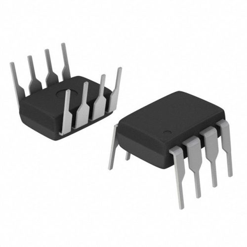
Overview: SN74LVC1G07 Open-Drain Buffer from Texas Instruments
"(《世界人权宣言》) SN74LVC1G07 从 德州仪器 is a single-channel buffer/driver with an open-drain output, designed for interfacing between mixed-voltage logic systems. It offers a versatile output structure that allows for pull-up resistor customization and multiple device connections.
Operating within a voltage range of 1.65V to 5.5V, the SN74LVC1G07 enables seamless signal buffering across different logic levels. Its support for high output impedance when disabled and low power consumption make it a reliable choice for industrial and embedded applications.
🔥 畅销产品
主要电气特性
| 参数 | 价值 | 单位 |
|---|---|---|
| 功能 | Open-Drain Buffer/Driver | – |
| 通道数 | 1 | – |
| 工作电压范围 | 1.65 ?C 5.5 | V |
| 输出类型 | Open-Drain | – |
| Input Type | CMOS | – |
| 包装 | SOT-23-5 | – |
| 最大传播延迟 | 5.2 | ns |
| ESD 保护 | 综合 | – |
Why SN74LVC1G07 is a Trusted Choice
The SN74LVC1G07 supports open-drain configuration, enabling efficient implementation of wired-AND logic functions, making it useful in communication buses like I2C or signal alert circuits. Unlike push-pull outputs, open-drain buffers provide higher design flexibility in multi-device environments.
This device delivers precise signal integrity even in compact layouts, thanks to its CMOS inputs and small SOT-23-5 footprint. Engineers rely on this device for its robust ESD protection, low power draw, and seamless compatibility across multiple voltage domains.
🌟 特色产品
Available now through 集成电路制造商, the SN74LVC1G07 ensures dependable signal control in resource-constrained industrial and consumer electronics designs.
技术参数和操作规格
| 特点 | 说明 |
|---|---|
| 逻辑家族 | LVC(低电压 CMOS) |
| Output Enable | No |
| Drive Capability | 24 毫安 |
| Static Power Consumption | 低 |
| 工作温度 | 摄氏 -40 度至 +125 度 |
| 安装 | Surface Mount (SOT-23-5) |
典型应用
- Signal buffering in digital logic systems
- Wired-AND logic buses (e.g., fault signals, interrupts)
- Voltage level interfacing in I2C-like communication
- Low-power monitoring systems and sensor interfaces
常见问题(FAQ)
What is the main purpose of SN74LVC1G07?
Its primary function is to buffer signals with an open-drain output, allowing integration in wired-AND logic and customized pull-up networks.
📩 联系我们
Is it suitable for high-speed communication?
Yes, the device offers fast propagation delays and is compatible with high-speed applications, particularly when controlling multiple devices via a shared bus.
Can I use it in a 3.3V to 5V interfacing circuit?
Absolutely. The operating voltage range of 1.65V to 5.5V ensures seamless compatibility with both 3.3V and 5V logic families.
What benefits does the SOT-23-5 package provide?
It saves PCB space, supports high-density assembly, and is ideal for modern miniature electronics.
Does it have power-saving features?
Yes. It is built on CMOS low-power technology and is optimized for low quiescent current, making it ideal for battery-powered systems.


