Overview: SN74LS137 High-Speed Address Decoder/Demux with Latch
"(《世界人权宣言》) SN74LS137 从 德州仪器 is a TTL logic device that integrates a 3-to-8 line decoder/demultiplexer with an internal address latch. It is optimized for high-speed memory decoding, enabling systems to expand their addressing capacity efficiently. The device allows the use of a latched input, helping in synchronization and timing-critical applications.
Capable of decoding three binary address inputs into eight mutually exclusive outputs, the SN74LS137 provides three separate enable inputs to control the activation of outputs. The device is widely used in memory addressing and I/O control logic where decoding flexibility is key.
🔥 畅销产品
Key Features and Logic Specifications
| 参数 | 价值 | 单位 |
|---|---|---|
| 功能 | 3-to-8 Decoder/Demultiplexer with Latch | – |
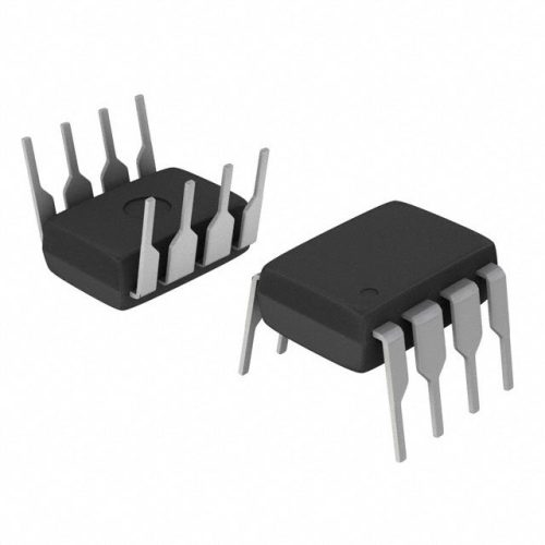
| 包装 | DIP-16 | – |
| Logic Type | TTL | – |
| Enable Inputs | 3 | – |
| Output Lines | 8 | – |
| Input Compatibility | TTL-Compatible | – |
| Output State | Active LOW | – |
| 安装类型 | Through Hole | – |
Advantages Over Standard 3-to-8 Decoders
Unlike basic decoders, the SN74LS137 includes an internal latch that retains address data, allowing input changes without affecting output states. This enhances timing control and reduces decoding errors in complex logic systems. Additionally, the three enable inputs provide extensive gating capabilities, allowing the device to be used in larger hierarchical or distributed decoder systems.
Its DIP-16 packaging supports through-hole assembly, beneficial for prototyping and industrial environments where mechanical reliability is crucial. Recommended by engineers for its robust performance and flexibility, the SN74LS137 is a cornerstone logic component in memory management and peripheral control systems.
🌟 特色产品
For industrial and embedded engineers sourcing reliable logic ICs, the SN74LS137 is now available from 集成电路制造商, a trusted supplier of digital and analog semiconductor components.
Technical Specifications Summary
| 特点 | 规格 |
|---|---|
| Address Inputs | 3-bit binary |
| Decoded Outputs | 8 mutually exclusive |
| Enable Inputs | 3 (G1 active HIGH, G2A/G2B active LOW) |
| Latch Enable | Active LOW |
| 传播延迟 | Typical ~22 ns |
| 输出类型 | Open-collector, active LOW |
| Input Compatibility | Standard TTL |
| 温度范围 | 0??C to 70??C |
| 安装 | Through-Hole (DIP-16) |
Typical Use Cases and Application Areas
- Memory chip select logic for microprocessor-based systems
- Address decoding in embedded controllers
- Peripheral selection in bus-oriented architectures
- Digital multiplexing and I/O port expansion
- Control systems with conditional logic gating
常见问题(FAQ)
What distinguishes the SN74LS137 from non-latching decoders?
It features an address latch, enabling stable output even when address inputs fluctuate. This is essential in systems where address transitions could cause instability without a latched state.
📩 联系我们
Can the SN74LS137 be used in memory-mapped I/O systems?
Yes. Its 3-to-8 decoding and enable inputs are perfectly suited for selecting specific memory or I/O blocks, reducing the need for external logic gates in microcontroller applications.
Is this IC compatible with standard 5V TTL logic?
Absolutely. The SN74LS137 is fully compatible with TTL levels, making it an excellent choice for older systems and modern logic designs that use 5V signaling.
Why are multiple enable inputs useful?
They allow the IC to be gated by multiple conditions. For instance, you can use one enable for timing, another for chip selection, and another for logic control, increasing circuit flexibility.
What packaging advantage does the DIP-16 offer?
DIP-16 is ideal for hand-soldering and prototyping on breadboards, as well as ensuring durable mounting in industrial systems where through-hole components are preferred for mechanical robustness.


