SN74HC595 Serial-In Parallel-Out Shift Register with Storage Register
O SN74HC595 is a widely adopted 8-bit serial-in, parallel-out shift register with tri-state output buffers, manufactured by Texas Instruments. This device is particularly suited for expanding the output capabilities of microcontrollers and embedded processors in space-constrained digital systems. Each register includes a storage register and a serial-to-parallel shift register, making it a reliable solution for efficient and synchronized output control in timing-sensitive applications.
With operation across a 2V to 6V power supply range, and outputs capable of sourcing or sinking TTL-level current, the SN74HC595 meets the voltage and current demands of most logic families. Through Fabricante de CI, verified component sourcing and consistent delivery are ensured, supporting the performance integrity in industrial-grade builds.
🔥 Produtos mais vendidos
-
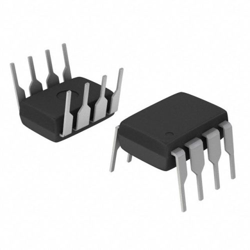
TLC555 Timer IC - Timer de Precisão da Texas Instruments em Pacote PDIP-8
-

Amplificador operacional de entrada JFET de baixo ruído TL081 da Texas Instruments - Pacote DIP-8
-

Controlador PWM de modo de corrente UC3842 da Texas Instruments - Pacote DIP-8
-

Texas Instruments LM2937 Regulador de Tensão Pacote TO-220 - Baixa Queda Linear
Electrical Characteristics and Performance Specifications
| Parâmetro | Valor | Unidade |
|---|---|---|
| Bits | 8 | – |
| Supply Voltage Range (Vcc) | 2 ?C 6 | V |
| Max Clock Frequency (at 6V) | 100 | MHz |
| Propagation Delay (tpd) | 15 (typ) | ns |
| Corrente de acionamento de saída | ??6 | mA |
| Tipo de embalagem | DIP-16 | – |
| Gama de temperaturas | -40 to +85 | ??C |
Advantages Over Conventional Output Expansion Techniques
- Integrated Storage Register: Allows output latching independent of shift register operation, minimizing flicker in LED arrays.
- Tri-State Outputs: Simplifies bus integration by allowing multiple ICs on the same data line.
- Flexible Voltage Operation: Compatible with both low-power 3.3V and standard 5V logic families.
- Compact Implementation: Reduces GPIO requirements while expanding output capacity by 8 bits per IC.
- Fast Propagation Time: Supports high-speed serial input up to 100 MHz for rapid state updates.
Technical Parameter Table
| Caraterística | Descrição |
|---|---|
| Função | Serial-In Parallel-Out Shift Register with Output Latch |
| Tipo de saída | Tri-State |
| Data Output Control | Storage Register + OE Pin |
| Clock Type | Positive-Edge Triggered |
| Fonte de alimentação | 2V to 6V |
| Output Enable | Active LOW |
| Família lógica | HC CMOS |
Aplicações típicas
- Microcontroller I/O Port Expansion
- LED Segment and Matrix Displays
- Industrial Control Panels
- Digital Interface Multiplexers
- Sistemas de aquisição de dados
Perguntas frequentes (FAQ)
What is the core purpose of the SN74HC595?
The SN74HC595 expands microcontroller I/O by converting a serial data stream into an 8-bit parallel output. It helps conserve GPIO pins while providing precise output control.
Can the SN74HC595 chips be cascaded for more outputs?
Yes, the devices can be chained via their QH?? and SER pins, allowing for nearly unlimited parallel expansion in 8-bit increments.
🌟 Produtos em destaque
-

"Comprar MAX9312ECJ+ Comparador de Tensão de Precisão em Pacote DIP para um Desempenho Fiável"
-
QCC-711-1-MQFN48C-TR-03-1 Bluetooth Audio SoC with MQFN48C Package
-

Modelo 0339-671-TLM-E - Pacote TLM-E de alto desempenho para funcionalidade aprimorada
-
1-1415898-4 Caixa do conetor, fio elétrico para placa, recetáculo, embalado
What is the benefit of the internal storage register?
It enables outputs to be updated simultaneously after all bits are shifted in, which is crucial for controlling displays and avoiding unwanted intermediate states.
How is data transferred into and out of the IC?
Data enters serially via the SER pin and shifts on the rising edge of the clock (SRCLK). The data is then latched to the outputs using the RCLK pin.
📩 Contactar-nos
What package options are available?
SN74HC595 is available in DIP-16, SOIC, and TSSOP formats, with DIP being ideal for through-hole applications and prototyping purposes.


