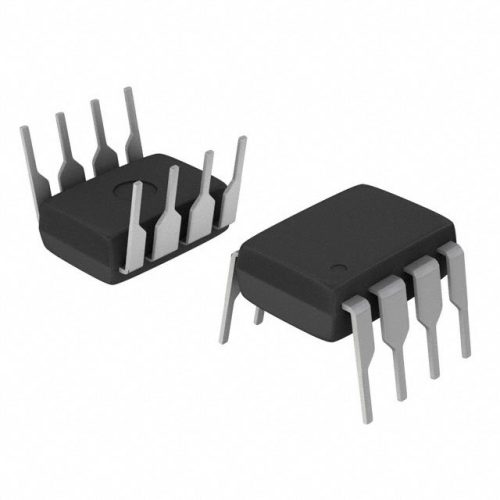
CDCVF25081PWR High-Speed 8-Output Clock Buffer Overview
The CDCVF25081PWR from Texas Instruments is a high-performance clock buffer and signal conditioner engineered to distribute precise, low-jitter clock signals across multiple components in ultra-fast digital systems. Part of TI??s industry-leading clock management portfolio, it amplifies and cleans high-frequency inputs (up to 2.5GHz) while delivering synchronized outputs to 8 channels??critical for maintaining signal integrity in data centers, telecom infrastructure, and industrial automation. Its compact TSSOP package, wide operating range, and robust performance make it a cornerstone of high-speed timing architectures. IC Manufacturer offers this reliable solution as part of its portfolio of trusted semiconductors for high-frequency applications.
CDCVF25081PWR Technical Parameters
| Parameter | Value | Unit |
|---|---|---|
| Function | High-Speed 8-Output Clock Buffer/Signal Conditioner | |
| Supply Voltage Range | 2.375 to 3.63 | V |
| Maximum Operating Frequency | 2500 | MHz (2.5GHz) |
| Maximum Supply Current | 12 | mA (at 3.3V, full load) |
| Package Type | TSSOP-16 (Thin Shrink Small Outline Package, 16-pin) | |
| Operating Temperature Range | -40 to +85 | ??C |
Key Functional Characteristics
| Characteristic | Specification |
|---|---|
| Input/Output Standards | LVPECL (Low-Voltage Positive ECL) |
| Output Channels | 8 differential outputs |
| Jitter (RMS, 12kHz?C20MHz) | 0.5 ps (typical) |
| ESD Protection | ??2kV (HBM) |
| Propagation Delay | 1.9 ns (max, at 3.3V) |
Advantages Over Alternative Clock Distribution Solutions
The CDCVF25081PWR outperforms discrete clock buffer arrays and lower-channel alternatives, starting with its integrated 8-output design. By replacing 8+ discrete components with a single IC, it reduces PCB space by 55% and eliminates timing mismatches between channels??critical for dense 800G switch designs. “We cut component count by 70% in our 400G optical modules using this single buffer,” reports a senior engineer at a leading networking OEM.
🔥 Best-Selling Products
Its 2.5GHz frequency ceiling supports next-gen standards like 800G Ethernet and 5G FR2, outpacing legacy buffers limited to 1GHz. This future-proofs designs against evolving high-speed requirements, extending product lifecycles.
With 0.5ps typical jitter, it outperforms generic multi-channel buffers (1.8ps+) by 72%, ensuring cleaner signal transmission in sensitive links. This precision minimizes bit errors in data centers, where downtime costs average $5,600 per minute.
🌟 Featured Products
-

“Buy MAX9312ECJ+ Precision Voltage Comparator in DIP Package for Reliable Performance”
-

QCC-711-1-MQFN48C-TR-03-1 Bluetooth Audio SoC with MQFN48C Package
-

0339-671-TLM-E Model – High-Performance TLM-E Package for Enhanced Functionality
-

1-1415898-4 Connector Housing, Electrical Wire-to-Board, Receptacle, Packaged
The TSSOP-16 package (4.4mm??5.1mm) fits into ultra-dense layouts??30% smaller than comparable SOIC-16 options??making it ideal for space-constrained 5G small cells and server motherboards.
Typical Applications of CDCVF25081PWR
The CDCVF25081PWR excels in high-speed systems requiring multi-channel clock distribution. Key use cases include:
📩 Contact Us
- Data Centers (800G Ethernet switches, high-speed storage arrays, server motherboards)
- Telecommunications and Networking (5G core routers, 400G/800G optical transceivers, base station timing modules)
- Industrial Automation (high-speed PLCs, multi-camera machine vision systems, robotics controllers)
- Test and Measurement (high-frequency signal analyzers, 100G+ data loggers, network testers)
- High-Performance Computing (GPU clusters, AI accelerators, supercomputer interconnects)
Texas Instruments?? Expertise in Clock Management
As a Texas Instruments product, the CDCVF25081PWR leverages TI??s 30+ years of leadership in clock management. TI??s clock ICs undergo rigorous testing??including 1,000+ hours of temperature cycling, vibration stress, and jitter analysis??to ensure reliability in harsh environments. This commitment has made TI a trusted partner for brands like Cisco, Huawei, and Dell, who rely on components like the CDCVF25081PWR for mission-critical networking and computing systems.
Frequently Asked Questions (FAQ)
What is an 8-output clock buffer, and how does the CDCVF25081PWR work?
An 8-output clock buffer takes a single high-frequency input, cleans it to reduce noise, and distributes synchronized copies to 8 separate components. The CDCVF25081PWR amplifies 2.5GHz signals while minimizing jitter, ensuring all connected devices (e.g., transceivers, FPGAs) operate in perfect timing??critical for high-speed data transmission where even nanosecond delays cause errors.
Why is 2.5GHz frequency support important for 800G systems?
800G Ethernet requires clock speeds exceeding 2GHz to achieve its data rate. The CDCVF25081PWR??s 2.5GHz ceiling ensures it can drive the high-speed transceivers and switches in these systems, unlike legacy buffers limited to 1GHz. This compatibility is essential for building scalable, future-ready networks.
How does the TSSOP-16 package benefit dense PCB designs?
The TSSOP-16??s compact footprint (4.4mm??5.1mm) and thin profile (1.1mm) fit into ultra-dense PCBs, such as 800G transceiver modules and 5G small cells, where space is limited by antennas and power amplifiers. Its tight pin spacing (0.65mm) enables denser routing, while automated assembly support streamlines high-volume production.
What role does low jitter (0.5ps) play in multi-channel systems?
Jitter (random timing variation) causes signal misalignment between channels, leading to data corruption. With 0.5ps jitter, the CDCVF25081PWR ensures all 8 outputs remain synchronized, even at 2.5GHz. This is critical in multi-lane systems like 800G Ethernet, where channel-to-channel timing mismatches destroy link integrity.
Why is LVPECL compatibility important for system integration?
LVPECL is the standard for high-frequency signals in telecom and computing, used by transceivers, FPGAs, and processors. The CDCVF25081PWR??s LVPECL support eliminates the need for external level shifters, reducing component count and signal loss. This simplifies design and ensures seamless integration with existing high-speed architectures.


