Overview: SN74LVC1G48 ?C Buffer Logic IC with Open-Drain Output
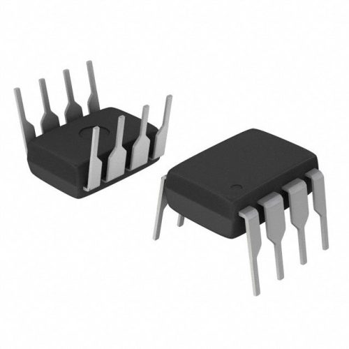
The SN74LVC1G48 from Texas Instruments is a high-performance CMOS logic buffer featuring an open-drain output and wide input voltage range. Designed for versatility, this device enables level translation and wired-logic configurations across modern electronic systems. The single non-inverting buffer supports flexible design implementation in systems requiring pull-up resistors or multi-point interconnection logic.
Encased in a compact SC-70-6 package, it meets the demand for space-efficient designs in portable and embedded systems. With its robust output drive and wide VCC support, the SN74LVC1G48 enhances both logic control and design reliability in high-density layouts.
🔥 Best-Selling Products
Technical Specifications Table
| Parameter | Min | Max | Unit |
|---|---|---|---|
| Supply Voltage (VCC) | 1.65 | 5.5 | V |
| Input Voltage Range | 0 | 5.5 | V |
| Output Type | Open-Drain | ?C | |
| Drive Strength | ??32 | ?C | mA |
| Package Type | SC-70-6 | ?C | |
| Operating Temp | -40 | 125 | ??C |
Why SN74LVC1G48 Outperforms Standard Buffers
Unlike typical push-pull buffers, this device features an open-drain configuration ideal for multi-voltage logic environments and wired-AND applications. It simplifies level shifting when paired with pull-up resistors, ensuring safe logic interfacing in mixed-voltage systems. The SC-70-6 package offers an optimal balance of performance and compact size. Available via IC Manufacturer, it reflects Texas Instruments’ high standards of logic reliability.
Extended Electrical Characteristics
| Feature | Specification |
|---|---|
| Logic Function | Non-inverting Buffer |
| Output Configuration | Open-Drain |
| Input Compatibility | TTL/CMOS |
| Quiescent Current | Low Static Power |
| Drive Capability | ??32 mA |
| Package | SC-70-6 |
| Temperature Range | ?C40??C to 125??C |
| Noise Margin | High |
Typical Applications
- Level shifting between different logic families
- Wired-AND logic for shared signal lines
- Signal buffering in I2C or other open-drain configurations
Frequently Asked Questions (FAQ)
What is the benefit of the open-drain output?
Open-drain allows for multiple outputs to share a single line using pull-up resistors, enabling wired-AND logic and level shifting in multi-voltage systems.
🌟 Featured Products
-

“Buy MAX9312ECJ+ Precision Voltage Comparator in DIP Package for Reliable Performance”
-

QCC-711-1-MQFN48C-TR-03-1 Bluetooth Audio SoC with MQFN48C Package
-

0339-671-TLM-E Model – High-Performance TLM-E Package for Enhanced Functionality
-

1-1415898-4 Connector Housing, Electrical Wire-to-Board, Receptacle, Packaged
Can the SN74LVC1G48 interface with both 3.3V and 5V systems?
Yes, it supports a wide operating range from 1.65V to 5.5V, making it compatible with both 3.3V and 5V logic levels.
Is this suitable for battery-powered applications?
Absolutely. With low quiescent current and efficient CMOS technology, it??s ideal for energy-sensitive systems such as wearables or handheld devices.
📩 Contact Us
How small is the SC-70-6 package?
The SC-70-6 footprint is optimized for minimal board usage, making it perfect for high-density and portable applications requiring reliable buffering logic.
Does this device support TTL logic levels?
Yes, the input thresholds are compatible with TTL and CMOS logic, providing design flexibility across mixed-signal platforms.


