MV2N4091-JFET-NChannel Overview
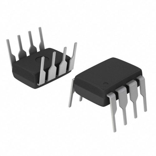
The MV2N4091 is a high-performance N-Channel JFET designed for low noise and high input impedance applications. With its robust electrical characteristics, this device excels in analog signal processing, sensor interfacing, and low-level amplification circuits. Its precise gate threshold voltage and stable operation under varying conditions make it ideal for precision electronic designs. Engineers and sourcing specialists will find this JFET suitable for industrial, instrumentation, and communications systems requiring reliable switching and amplification. For more detailed product insights and sourcing options, visit IC Manufacturer.
MV2N4091-JFET-NChannel Technical Specifications
| Parameter | Specification | Unit |
|---|---|---|
| Drain-Source Voltage (V_DS) | 30 | V |
| Gate-Source Cutoff Voltage (V_GS(off)) | -0.5 to -6.0 | V |
| Drain Current (I_D) | 5 | mA |
| Gate Reverse Current (I_GSS) | 10 | pA |
| Input Capacitance (C_iss) | 3 | pF |
| Transconductance (g_m) | 2.5 | mS |
| Noise Figure | Low | nV/??Hz |
| Operating Temperature Range | -55 to +150 | ??C |
MV2N4091-JFET-NChannel Key Features
- Low gate leakage current: Ensures minimal input signal distortion, critical for high-impedance sensor circuits.
- Wide gate-source cutoff voltage range: Provides design flexibility for various biasing conditions and application requirements.
- High transconductance: Enables efficient signal amplification with reduced power consumption, enhancing circuit performance.
- Stable operation across temperature extremes: Guarantees reliability in industrial and automotive environments.
Typical Applications
- Low-noise preamplifiers in audio and instrumentation systems, where signal integrity is paramount and low distortion is required.
- Analog switches and chopper amplifiers that benefit from the device??s low gate leakage and high input impedance.
- Sensor interfaces including photodiodes and strain gauges, where high input impedance and low noise enhance measurement accuracy.
- Current regulators and voltage-controlled resistors in precision analog circuits demanding stable operation and low power dissipation.
MV2N4091-JFET-NChannel Advantages vs Typical Alternatives
This N-Channel JFET offers superior low-noise performance and extremely low gate leakage currents compared to typical MOSFET or bipolar alternatives. Its wide operating voltage and temperature range provide robust reliability in challenging industrial environments. These advantages result in better signal fidelity, improved power efficiency, and enhanced long-term device stability, making it a preferred choice for precision analog and sensor applications.
🔥 Best-Selling Products
MV2N4091-JFET-NChannel Brand Info
The MV2N4091 is a product from a leading semiconductor manufacturer specializing in discrete components and analog devices. Known for their stringent quality control and reliable performance, the brand offers this JFET as part of their portfolio targeting industrial, instrumentation, and communication markets. The device benefits from established manufacturing processes and comprehensive datasheets, ensuring engineers have full technical support and sourcing confidence for demanding designs.
FAQ
What is the typical gate-source cutoff voltage range for this N-Channel JFET?
The gate-source cutoff voltage (V_GS(off)) typically ranges from -0.5 V to -6.0 V. This wide range allows designers to select appropriate biasing points depending on circuit requirements and desired operating characteristics.
🌟 Featured Products
-

“Buy MAX9312ECJ+ Precision Voltage Comparator in DIP Package for Reliable Performance”
-

QCC-711-1-MQFN48C-TR-03-1 Bluetooth Audio SoC with MQFN48C Package
-

0339-671-TLM-E Model – High-Performance TLM-E Package for Enhanced Functionality
-

1-1415898-4 Connector Housing, Electrical Wire-to-Board, Receptacle, Packaged
How does the low gate leakage current benefit analog signal applications?
Low gate leakage current minimizes input bias current, preserving signal integrity in high-impedance circuits. This is especially important in sensor interfacing and low-level amplification, where even small leakage can distort the signal or add noise.
Can this device operate reliably in extreme temperature conditions?
Yes, the device is rated for operation from -55??C to +150??C, making it suitable for industrial and automotive applications where


