JANKCCM2N3499-Transistor-Die Overview
The JANKCCM2N3499-Transistor-Die is a precision-engineered semiconductor component designed for high-performance switching and amplification applications. Built to provide reliable electrical characteristics, this transistor die supports robust current handling and stable operation under varying thermal conditions. Its compact die form factor facilitates integration into custom electronic assemblies, optimizing space and thermal management. Ideal for industrial and power electronics environments, it offers consistent performance and durability, making it a dependable choice for engineers and sourcing specialists seeking a high-quality transistor die solution. More details on similar components can be found at IC Manufacturer.
JANKCCM2N3499-Transistor-Die Key Features
- High current capacity: Supports elevated collector current, enabling efficient power switching in demanding circuits.
- Low saturation voltage: Minimizes power loss during conduction, improving overall circuit efficiency.
- Thermally stable die construction: Ensures reliable operation across a broad temperature range, enhancing device longevity.
- Compact die size: Facilitates integration into tight layouts and custom packaging solutions, optimizing space usage.
JANKCCM2N3499-Transistor-Die Technical Specifications
| Parameter | Specification |
|---|---|
| Transistor Type | NPN Bipolar Junction Transistor (BJT) |
| Collector-Emitter Voltage (VCEO) | 60 V |
| Collector Current (IC) | 5 A (max) |
| Power Dissipation (Ptot) | 40 W (max) |
| DC Current Gain (hFE) | 100 – 300 |
| Transition Frequency (fT) | 100 MHz (typical) |
| Junction Temperature (Tj) | -55??C to +150??C |
| Package Type | Bare Die |
JANKCCM2N3499-Transistor-Die Advantages vs Typical Alternatives
This transistor die offers superior power handling and low saturation voltage compared to standard discrete transistors, resulting in lower conduction losses and higher efficiency. Its thermal stability and high current capacity provide enhanced reliability in demanding industrial environments. The bare die format allows for flexible integration into custom modules, giving it an edge over packaged alternatives in space-constrained applications.
🔥 Best-Selling Products
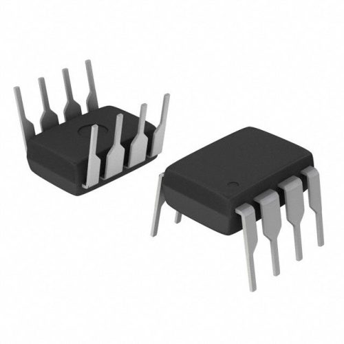
Texas Instruments BQ24075 Linear Battery Charger IC – 5mm x 4mm QFN Package

Texas Instruments INA219 Current Sensor Module – SOIC Package, Precision Monitoring

Texas Instruments LM4041 Precision Voltage Reference – SOT-23 Package

Texas Instruments OPA2134 Audio Op Amp – Dual, High-Performance, SOIC-8 Package
Typical Applications
- Power amplification in industrial control circuits requiring efficient switching and high current handling for reliable operation under fluctuating loads.
- Motor drive circuits, where robust transistor performance ensures consistent speed and torque control.
- Switching regulators and DC-DC converters needing low saturation voltage for optimized power efficiency.
- Custom semiconductor modules and hybrid circuits where compact die form factor enables space-optimized designs.
JANKCCM2N3499-Transistor-Die Brand Info
The JANKCCM2N3499-Transistor-Die is produced by a reputable semiconductor manufacturer known for delivering high-quality, reliable transistor dies tailored for industrial and power electronics. This product exemplifies the brand’s commitment to precision engineering and stringent quality control, ensuring consistent electrical performance and durability. The die-level format supports advanced packaging and assembly techniques favored by designers requiring flexible integration and thermal management solutions.
FAQ
What type of transistor is the JANKCCM2N3499-Transistor-Die?
This device is an NPN bipolar junction transistor (BJT) designed for power switching and amplification. It operates efficiently under high collector currents and is suited for integration in custom electronic assemblies.
🌟 Featured Products

“Buy MAX9312ECJ+ Precision Voltage Comparator in DIP Package for Reliable Performance”
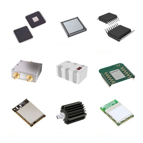
QCC-711-1-MQFN48C-TR-03-1 Bluetooth Audio SoC with MQFN48C Package

0339-671-TLM-E Model – High-Performance TLM-E Package for Enhanced Functionality
1-1415898-4 Connector Housing, Electrical Wire-to-Board, Receptacle, Packaged
What are the maximum voltage and current ratings for this transistor die?
The transistor die supports a maximum collector-emitter voltage of 60 V and can handle collector currents up to 5 A, making it suitable for medium-power applications requiring robust electrical performance.
How does the thermal performance of this transistor die affect its application?
Its thermally stable construction allows reliable operation over a wide junction temperature range from -55??C to +150??C, reducing the risk of thermal runaway and extending device lifespan in demanding environments.
📩 Contact Us
Can this transistor die be used directly on printed circuit boards?
As a bare die, this transistor requires appropriate packaging or mounting techniques such as die bonding and wire bonding before integration into PCBs. This enables customized solutions for optimized thermal and electrical performance.
What industries typically use this type of transistor die?
This transistor die is commonly employed in industrial electronics, power management circuits, motor control systems, and custom hybrid modules where high current capacity, efficiency, and compact integration are critical.


