JANKCCH2N3499-Transistor-Die Overview
The JANKCCH2N3499-Transistor-Die is a high-performance semiconductor component designed for precision amplification and switching applications. Its compact die form factor allows direct integration into custom IC packages and hybrid modules, optimizing space while maintaining excellent electrical characteristics. Featuring robust current handling and reliable thermal stability, this transistor die is suitable for high-frequency and power-sensitive environments. Engineers and sourcing specialists benefit from its consistent quality and compatibility with various assembly processes. For detailed manufacturing standards and procurement options, visit IC Manufacturer.
JANKCCH2N3499-Transistor-Die Key Features
- High Current Gain: Delivers efficient signal amplification, ensuring improved circuit performance in demanding applications.
- Low Saturation Voltage: Minimizes power loss during switching, enhancing overall system energy efficiency.
- Thermal Stability: Maintains consistent operation across a broad temperature range, critical for industrial reliability.
- Compact Die Size: Enables flexible integration into custom semiconductor packages and complex assembly designs.
JANKCCH2N3499-Transistor-Die Technical Specifications
| Parameter | Specification |
|---|---|
| Type | NPN Bipolar Junction Transistor (BJT) |
| Collector-Emitter Voltage (Vceo) | 60 V |
| Collector Current (Ic) | 5 A (max) |
| Power Dissipation (Pd) | 40 W (max) |
| Current Gain (hFE) | 100 ?C 300 |
| Transition Frequency (fT) | 100 MHz (typical) |
| Packaging | Bare Die |
| Operating Temperature Range | -55??C to +150??C |
| Base-Emitter Voltage (Vbe) | 1.2 V (typical) |
JANKCCH2N3499-Transistor-Die Advantages vs Typical Alternatives
This transistor die offers superior current handling and thermal stability compared to typical discrete transistors, making it ideal for high-reliability applications. Its low saturation voltage reduces power dissipation, enhancing system efficiency. The bare die format supports flexible integration into advanced packaging solutions, providing a distinct advantage in miniaturized and high-density circuit designs.
🔥 Best-Selling Products
Typical Applications
- Power Amplification in RF circuits where high gain and frequency response are critical for signal integrity and system performance.
- Switching components in industrial motor control systems requiring robust current capacity and thermal reliability.
- Integration into hybrid modules for automotive electronics demanding high endurance under thermal stress.
- Custom semiconductor assemblies used in telecommunications infrastructure for stable, high-frequency operation.
JANKCCH2N3499-Transistor-Die Brand Info
The JANKCCH2N3499-Transistor-Die is produced by a leading semiconductor manufacturer specializing in advanced die-level transistor technologies. This product exemplifies the brand??s commitment to delivering reliable, high-performance components tailored for demanding industrial and communications markets. The brand??s expertise ensures consistent quality control and adherence to semiconductor industry standards, supporting innovative electronic designs worldwide.
FAQ
What type of transistor is the JANKCCH2N3499-Transistor-Die?
The device is an NPN bipolar junction transistor (BJT) delivered in bare die form. It is designed for applications requiring efficient switching and amplification within a compact semiconductor package.
🌟 Featured Products
-

“Buy MAX9312ECJ+ Precision Voltage Comparator in DIP Package for Reliable Performance”
-
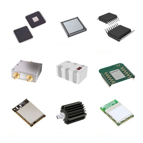
QCC-711-1-MQFN48C-TR-03-1 Bluetooth Audio SoC with MQFN48C Package
-

0339-671-TLM-E Model – High-Performance TLM-E Package for Enhanced Functionality
-
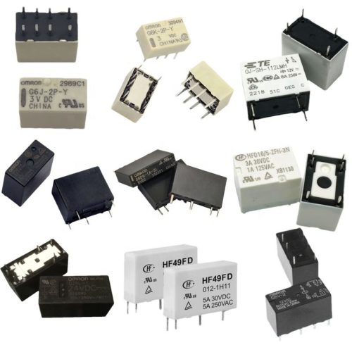
1-1415898-4 Connector Housing, Electrical Wire-to-Board, Receptacle, Packaged
What is the maximum collector current this transistor die can handle?
This transistor die supports a maximum collector current of 5 amperes, making it suitable for medium-power applications where reliable current flow is essential.
How does the die format benefit system integration?
The bare die format allows direct mounting and wire bonding within custom IC packages or hybrid modules. This flexibility supports compact designs and improved thermal management not achievable with standard packaged transistors.
📩 Contact Us
What temperature range can this transistor die operate within?
The device maintains reliable performance across a wide operating temperature range from -55??C up to +150??C, ensuring suitability for harsh industrial and automotive environments.
What is the typical current gain (hFE) of this transistor die?
The typical current gain ranges from 100 to 300, providing strong amplification characteristics that enhance signal processing in various electronic circuits.


