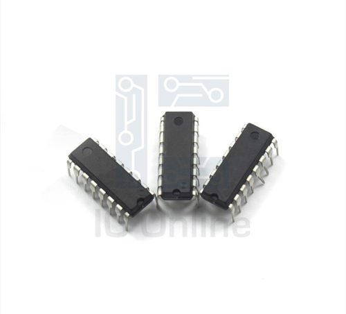
JANKCCF2N5151-Transistor-Die Overview
The JANKCCF2N5151-Transistor-Die is a high-performance NPN bipolar junction transistor die designed for integration into semiconductor devices requiring precise switching and amplification functions. This transistor die delivers robust electrical characteristics, including a maximum collector current of 150mA and a collector-emitter voltage rating of 50V, making it suitable for medium-power applications. The die format enables seamless integration into custom chip assemblies or multi-chip modules, optimizing circuit density and performance. Its reliable gain and frequency response characteristics ensure efficient signal processing in industrial electronics. Sourcing specialists and engineers benefit from its stable electrical parameters and compatibility with diverse manufacturing workflows. For detailed IC component sourcing, visit IC Manufacturer.
JANKCCF2N5151-Transistor-Die Technical Specifications
| Parameter | Value | Unit |
|---|---|---|
| Type | NPN Bipolar Junction Transistor | ?? |
| Collector-Emitter Voltage (VCEO) | 50 | V |
| Collector-Base Voltage (VCBO) | 60 | V |
| Emitter-Base Voltage (VEBO) | 5 | V |
| Collector Current (IC) | 150 | mA |
| Power Dissipation (Ptot) | 400 | mW |
| DC Current Gain (hFE) | 100 – 300 | ?? |
| Transition Frequency (fT) | 100 | MHz |
| Package Style | Die (bare silicon chip) | ?? |
JANKCCF2N5151-Transistor-Die Key Features
- High voltage handling: Supports collector-emitter voltages up to 50V, enabling use in medium-voltage switching applications with enhanced reliability.
- Robust collector current capacity: Allows continuous collector currents of 150mA, suitable for moderate power amplification and switching tasks in industrial electronics.
- Wide gain range: DC current gain between 100 and 300 ensures flexibility for different amplification requirements and circuit designs.
- High transition frequency: Operating up to 100MHz, the transistor die is optimized for high-frequency analog signal processing and switching efficiency.
- Die form factor: Enables direct integration into multi-chip modules or custom semiconductor packages, allowing designers to optimize layout and minimize parasitic effects.
- Low power dissipation: Maximum power rating of 400mW supports energy-efficient circuit design and thermal management.
Typical Applications
- Signal amplification in medium-frequency analog circuits, where precise gain and low distortion are critical for system performance.
- Switching elements in power management circuits, leveraging the transistor??s voltage and current ratings for reliable operation.
- Integration in multi-chip modules for industrial control systems requiring compact, high-performance transistor components.
- Use in driver stages for relay or small motor control circuits, offering stable current handling and switching speed.
JANKCCF2N5151-Transistor-Die Advantages vs Typical Alternatives
This transistor die offers a balanced combination of voltage rating, current capacity, and frequency response that outperforms many generic transistor dies in its class. Its bare die format allows tighter integration into advanced semiconductor assemblies, reducing parasitic effects and improving overall circuit performance. Compared to packaged transistors, this die enables greater flexibility for custom solutions, enhancing reliability and thermal management in industrial applications.
🔥 Best-Selling Products
Texas Instruments BQ24075 Linear Battery Charger IC – 5mm x 4mm QFN Package

Texas Instruments INA219 Current Sensor Module – SOIC Package, Precision Monitoring

Texas Instruments LM4041 Precision Voltage Reference – SOT-23 Package

Texas Instruments OPA2134 Audio Op Amp – Dual, High-Performance, SOIC-8 Package


