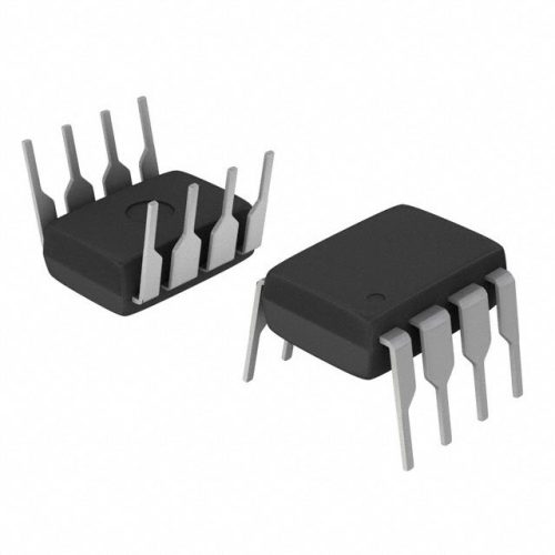
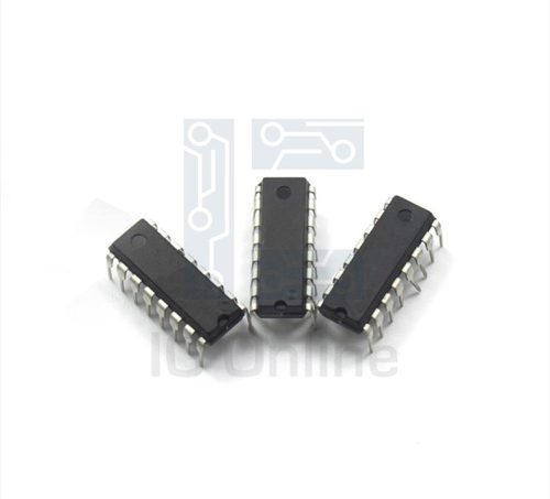
JANKCBP2N2222A-Transistor-Die Overview
The JANKCBP2N2222A-Transistor-Die is a high-performance NPN bipolar junction transistor die designed for versatile switching and amplification applications. Offering robust current gain and reliable operation at moderate voltages, this transistor die is ideal for integration into compact, high-density semiconductor modules. The device ensures efficient electron mobility and stable thermal characteristics, making it suitable for demanding industrial electronics and signal processing tasks. Available from IC Manufacturer, this transistor die supports engineers and sourcing specialists seeking dependable, precision semiconductor components for custom circuit design and manufacturing.
JANKCBP2N2222A-Transistor-Die Technical Specifications
| Parameter | Value |
|---|---|
| Type | NPN Bipolar Junction Transistor (BJT) Die |
| Collector-Emitter Voltage (VCEO) | 40 V |
| Collector Current (IC) | 800 mA (max) |
| Power Dissipation (Ptot) | 625 mW (die level) |
| DC Current Gain (hFE) | 100 to 300 (typical) |
| Transition Frequency (fT) | 250 MHz (typical) |
| Package Type | Unpackaged Die (bare silicon) |
| Operating Temperature Range | -55??C to +150??C |
| Base-Emitter Voltage (VBE) | 0.7 V (typical at 10 mA) |
JANKCBP2N2222A-Transistor-Die Key Features
- High current gain: Enables efficient signal amplification with minimal input current, improving overall circuit sensitivity.
- Robust voltage handling: Supports collector-emitter voltages up to 40 V, suitable for moderate voltage switching applications.
- Compact die form factor: Facilitates integration into custom semiconductor packages and modules, optimizing space utilization.
- Wide operating temperature range: Ensures reliable performance in harsh environments from -55??C to +150??C.
- High transition frequency: Supports fast switching speeds up to 250 MHz, beneficial for high-frequency circuit designs.
- Low base-emitter voltage drop: Minimizes power consumption during transistor operation, enhancing energy efficiency.
- Unpackaged die: Offers flexibility for advanced packaging and assembly processes in semiconductor manufacturing.
Typical Applications
- Signal amplification in low to medium power analog circuits, where precise gain and linearity are critical for performance.
- Switching devices in industrial control systems requiring reliable operation under varying load conditions.
- Driver transistors in relay and solenoid control circuits, providing efficient current switching capability.
- High-frequency oscillator and amplifier stages in communication equipment, benefiting from fast transition frequency.
JANKCBP2N2222A-Transistor-Die Advantages vs Typical Alternatives
This transistor die offers a balance of high current gain and moderate voltage tolerance that stands out compared to typical discrete transistors. Its unpackaged bare die format allows engineers to implement custom packaging solutions, achieving better thermal management and integration in high-density assemblies. The wide operating temperature range and consistent switching performance provide enhanced reliability over common transistor alternatives, making it a preferred choice for demanding industrial and communication applications.
🔥 Best-Selling Products
JANKCBP2N2222A-Transistor-Die Brand Info
The JANKCBP2N2222A transistor die is associated with established semiconductor manufacturers specializing in high-quality silicon discrete components. Known for its consistent electrical characteristics and reliability, this device is widely recognized in the industry as a foundational NPN transistor die. Its design roots trace back to the classic 2N2222 transistor family, refined for bare die applications to support custom semiconductor packaging and integration. This product aligns with the standards expected from leading IC manufacturers focused on industrial and signal processing solutions.
FAQ
What is the maximum collector current rating of this transistor die?
The maximum collector current for this transistor die is rated at 800 mA. This current limit
🌟 Featured Products
-

“Buy MAX9312ECJ+ Precision Voltage Comparator in DIP Package for Reliable Performance”
-
QCC-711-1-MQFN48C-TR-03-1 Bluetooth Audio SoC with MQFN48C Package
-

0339-671-TLM-E Model – High-Performance TLM-E Package for Enhanced Functionality
-
1-1415898-4 Connector Housing, Electrical Wire-to-Board, Receptacle, Packaged


