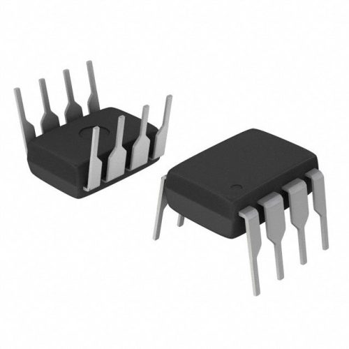
JANKCA2N3637-Transistor-Die Overview
The JANKCA2N3637-Transistor-Die is a high-performance semiconductor component designed for robust amplification and switching applications. Its die-level construction allows for direct integration into custom circuits, providing engineers with precise control over electrical characteristics. Featuring a reliable transistor architecture, this die supports efficient current handling with optimized gain and switching speed. Ideal for industrial and electronic system designers, the device delivers consistent performance in demanding environments. For detailed technical and sourcing information, refer to IC Manufacturer.
JANKCA2N3637-Transistor-Die Key Features
- High current capacity: Supports substantial collector current, enabling effective power amplification in compact form.
- Optimized gain characteristics: Ensures precise control and signal amplification critical for analog and switching circuits.
- Compact die size: Facilitates integration into custom semiconductor packages or modules, improving design flexibility.
- Thermal robustness: Designed to operate reliably under elevated temperatures, enhancing system durability.
JANKCA2N3637-Transistor-Die Technical Specifications
| Parameter | Specification |
|---|---|
| Type | Bipolar Junction Transistor (BJT) Die |
| Collector-Emitter Voltage (VCEO) | 60 V |
| Collector Current (IC) | 6 A |
| Power Dissipation (PD) | 40 W (die level) |
| Gain Bandwidth Product (fT) | 80 MHz |
| DC Current Gain (hFE) | 40 to 320 (varies by operating point) |
| Junction Temperature (TJ) | Up to 150??C |
| Package Type | Bare Die (for integration) |
JANKCA2N3637-Transistor-Die Advantages vs Typical Alternatives
This transistor die offers enhanced current handling and thermal endurance compared to typical packaged devices. Its bare die format provides engineers with superior flexibility for custom module integration, enabling optimized thermal management and reduced parasitic losses. The device??s gain and frequency response facilitate precise analog amplification and fast switching, making it a reliable choice for high-performance industrial applications.
🔥 Best-Selling Products
Typical Applications
- Power amplification in industrial control and analog signal processing circuits, where reliable current capacity and gain stability are essential for system performance.
- Switching elements in high-frequency power supplies and converters, leveraging fast response times and thermal robustness.
- Custom semiconductor module assembly, allowing integration into multi-chip packages for space-constrained environments.
- Embedded transistor arrays in mixed-signal systems requiring precise amplification and switching functions.
JANKCA2N3637-Transistor-Die Brand Info
The JANKCA2N3637-Transistor-Die is produced by a trusted semiconductor manufacturer known for delivering high-quality transistor components aimed at industrial and advanced electronics applications. This die reflects the brand??s commitment to precision engineering and reliability, supporting designers and engineers in creating custom solutions with enhanced electrical performance and durability.
FAQ
What is the maximum collector current rating of this transistor die?
The transistor die supports a maximum collector current of 6 amperes, making it suitable for applications requiring moderate to high power levels while maintaining stable operation.
🌟 Featured Products
-

“Buy MAX9312ECJ+ Precision Voltage Comparator in DIP Package for Reliable Performance”
-
QCC-711-1-MQFN48C-TR-03-1 Bluetooth Audio SoC with MQFN48C Package
-

0339-671-TLM-E Model – High-Performance TLM-E Package for Enhanced Functionality
-
1-1415898-4 Connector Housing, Electrical Wire-to-Board, Receptacle, Packaged
Can this die be used in high-frequency switching circuits?
Yes, with a gain bandwidth product of approximately 80 MHz, this transistor die is well-suited for switching applications that demand fast response and reliable signal amplification.
How does the bare die format benefit system designers?
The bare die format allows engineers to integrate the transistor directly into custom semiconductor packages or modules, enabling improved thermal management and reduced electrical parasitics compared to standard packaged devices.
📩 Contact Us
What is the operating temperature range for this transistor die?
The device is rated for junction temperatures up to 150??C, ensuring robust performance in environments with elevated temperatures common in industrial electronics.
What kind of applications is this transistor die typically used for?
It is commonly employed in power amplifiers, switching power supplies, custom module assemblies, and embedded circuits where precise current control and thermal reliability are critical.


