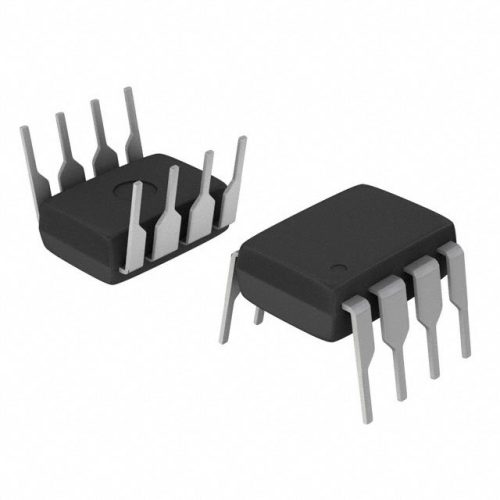
JAN2N5662-Transistor Overview
The JAN2N5662 transistor is a high-performance bipolar junction transistor (BJT) designed to deliver reliable switching and amplification in demanding industrial and military applications. Featuring a silicon NPN construction, it offers robust electrical characteristics including high voltage and current handling capabilities. This transistor is well-suited for use in power amplification, signal processing, and other electronic circuits requiring stable operation under varied conditions. Manufactured to meet stringent military standards, it ensures consistent performance and durability. For engineers and sourcing specialists seeking a dependable transistor for critical designs, this component from IC Manufacturer stands out as a solid choice.
JAN2N5662-Transistor Key Features
- High voltage rating: Supports collector-emitter voltages up to 80V, enabling operation in circuits requiring robust voltage tolerance.
- Substantial collector current: Can handle collector currents up to 5A, suitable for power amplification and switching tasks.
- Military-grade reliability: Built to meet JAN (Joint Army-Navy) standards, ensuring superior durability and dependable operation in harsh environments.
- Low saturation voltage: Enhances switching efficiency by minimizing power loss during transistor saturation.
JAN2N5662-Transistor Technical Specifications
| Parameter | Value | Unit |
|---|---|---|
| Transistor Type | NPN | |
| Collector-Emitter Voltage (Vceo) | 80 | V |
| Collector-Base Voltage (Vcbo) | 100 | V |
| Emitter-Base Voltage (Vebo) | 5 | V |
| Collector Current (Ic) | 5 | A |
| Power Dissipation (Pc) | 30 | W |
| DC Current Gain (hFE) | 40 – 160 | |
| Transition Frequency (fT) | 5 | MHz |
| Operating Temperature Range | -65 to +200 | ??C |
JAN2N5662-Transistor Advantages vs Typical Alternatives
This transistor provides a compelling advantage through its combination of high voltage tolerance and substantial current capacity, which many standard BJTs cannot match simultaneously. Its military-grade certification ensures enhanced reliability and longevity, making it ideal for applications where failure is not an option. Additionally, the device??s low saturation voltage improves energy efficiency compared to typical power transistors, leading to reduced thermal stress and improved circuit performance.
🔥 Best-Selling Products
Typical Applications
- Power amplification in industrial and military communication systems, where stable gain and high voltage handling are essential for signal integrity.
- Switching circuits within control and regulation modules, benefiting from its fast switching and low saturation voltage characteristics.
- Driver stages for motors and solenoids, leveraging the device??s ability to manage significant collector currents.
- General-purpose amplification and switching in ruggedized electronics requiring operation over a wide temperature range.
JAN2N5662-Transistor Brand Info
The JAN2N5662 transistor is part of a series manufactured under the rigorous Joint Army-Navy (JAN) standards, reflecting a commitment to quality and reliability. This product is designed and tested to endure extreme environmental and electrical stresses, making it a trusted choice for defense and aerospace sectors. Backed by a reputable semiconductor manufacturer, it combines proven design with strict quality control, ensuring consistent performance for demanding applications.
FAQ
What is the maximum collector current the JAN2N5662 can handle?
The transistor can handle a maximum collector current of 5 amperes, allowing it to be used in power amplification and switching applications where substantial current capacity is required.
🌟 Featured Products
-

“Buy MAX9312ECJ+ Precision Voltage Comparator in DIP Package for Reliable Performance”
-
QCC-711-1-MQFN48C-TR-03-1 Bluetooth Audio SoC with MQFN48C Package
-

0339-671-TLM-E Model – High-Performance TLM-E Package for Enhanced Functionality
-
1-1415898-4 Connector Housing, Electrical Wire-to-Board, Receptacle, Packaged
What voltage ratings does this transistor support?
This device supports a collector-emitter voltage (Vceo) of up to 80 volts, a collector-base voltage (Vcbo) up to 100 volts, and an emitter-base voltage (Vebo) of 5 volts, suitable for high-voltage operating environments.
How does the JAN2N5662 ensure reliability in harsh conditions?
Manufactured according to strict JAN military standards, the transistor undergoes rigorous testing for temperature extremes, electrical stress, and mechanical durability, ensuring reliable operation in demanding industrial and defense applications.
📩 Contact Us
What is the typical DC current gain range for this transistor?
The DC current gain (hFE) typically ranges from 40 to 160, providing flexibility for various amplification requirements while maintaining stable performance within its operating conditions.
Is the JAN2N5662 suitable for high-frequency applications?
With a transition frequency (fT) of approximately 5 MHz, this transistor is suited for moderate frequency applications, including audio and low RF stages, but may not be optimal for very high-frequency circuits.


