CY7C199-35SI Overview
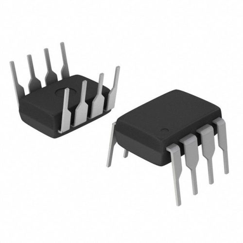
The CY7C199-35SI is a high-performance 4K x 9-bit static RAM designed for fast and reliable data storage in industrial and embedded applications. Operating at a 35 ns access time, this SRAM ensures swift read and write cycles essential for real-time processing. Its low power consumption combined with a standardized JEDEC-compatible footprint makes it ideal for system designers seeking efficient memory solutions. With a straightforward asynchronous interface, the device supports seamless integration into various digital systems, enhancing overall application performance. For sourcing and technical details, visit IC Manufacturer.
CY7C199-35SI Technical Specifications
| Parameter | Specification |
|---|---|
| Memory Size | 4K x 9 bits |
| Access Time | 35 ns |
| Operating Voltage | 5 V ?? 10% |
| Data Retention Voltage | 2 V minimum |
| Power Supply Current (Active) | 40 mA (max) |
| Power Supply Current (Standby) | 10 mA (max) |
| Package Type | 28-pin SOJ |
| Temperature Range | 0??C to +70??C (Commercial) |
| Interface | Asynchronous |
| Data I/O | 9-bit |
CY7C199-35SI Key Features
- Fast 35 ns access time: Enables rapid data retrieval and storage, critical for time-sensitive applications.
- 4K x 9-bit organization: Provides flexible data width and storage capacity suitable for various embedded systems.
- Low power consumption: Optimized for minimal active and standby current, enhancing energy efficiency in battery-powered or low-power environments.
- Standard 28-pin SOJ package: Ensures compatibility with existing PCB layouts and simplifies system integration.
- Asynchronous SRAM interface: Allows easy interfacing without requiring complex timing controls, reducing design complexity.
- Reliable data retention voltage: Maintains memory contents even with reduced power supply levels, supporting system stability during power fluctuations.
- Commercial temperature range: Suitable for a wide range of operating environments typical in industrial and commercial applications.
CY7C199-35SI Advantages vs Typical Alternatives
This SRAM offers a superior balance of speed and low power consumption compared to typical asynchronous static RAMs. Its 35 ns access time ensures faster data throughput, while the 9-bit data width supports wider data paths than standard 8-bit devices. The device??s stable operation across commercial temperature ranges and compliance with JEDEC standards make it a reliable and easy-to-integrate memory choice for engineers prioritizing performance and system compatibility.
🔥 Best-Selling Products
Typical Applications
- Embedded systems requiring fast, low-latency memory for buffering and temporary data storage in industrial automation and control equipment.
- High-speed data acquisition systems where quick access to stored data supports real-time processing and analysis.
- Communication devices that need rapid memory access for protocol handling and data buffering tasks.
- Consumer electronics with moderate memory requirements where power efficiency and fast operation improve overall device responsiveness.
CY7C199-35SI Brand Info
The CY7C199-35SI is part of Cypress Semiconductor??s well-established family of high-speed static RAM products. Known for robust design and reliable performance, this device embodies Cypress??s commitment to providing memory solutions that meet the demands of industrial and embedded applications. Engineered for ease of integration and sustained performance, it supports developers and sourcing specialists in achieving optimized system designs with proven semiconductor technology.
FAQ
What is the access time specification for this SRAM?
The access time is 35 nanoseconds, which defines the maximum delay between the address input and valid data output. This fast access speed supports applications needing quick memory reads and writes.
🌟 Featured Products
-

“Buy MAX9312ECJ+ Precision Voltage Comparator in DIP Package for Reliable Performance”
-

QCC-711-1-MQFN48C-TR-03-1 Bluetooth Audio SoC with MQFN48C Package
-

0339-671-TLM-E Model – High-Performance TLM-E Package for Enhanced Functionality
-

1-1415898-4 Connector Housing, Electrical Wire-to-Board, Receptacle, Packaged
What power supply voltage does the device require?
The SRAM operates at a nominal 5 volts supply with a tolerance of ??10%. It also supports data retention down to 2 volts, allowing it to maintain stored data during low power conditions.


