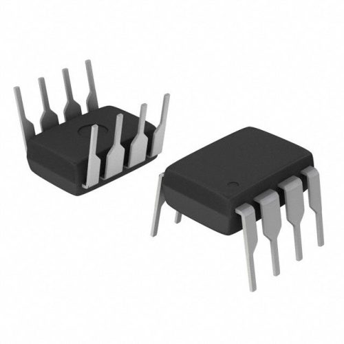
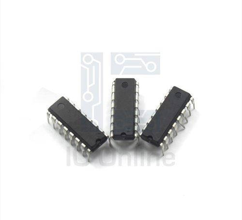
CD5314 Overview
The CD5314 is a CMOS digital logic device designed for industrial and commercial applications requiring reliable logic functions with low power consumption. This integrated circuit operates with a wide supply voltage range and offers high noise immunity, making it suitable for robust system designs. Its stable switching characteristics ensure predictable performance in various environments. The device is manufactured by IC Manufacturer, known for quality semiconductor solutions tailored to meet demanding industrial requirements.
CD5314 Technical Specifications
| Parameter | Specification |
|---|---|
| Supply Voltage (VDD) | 3 V to 15 V |
| Input Voltage Range | 0 V to VDD |
| Maximum Operating Frequency | Up to 10 MHz (typical) |
| Power Dissipation | Low power CMOS technology |
| Input Current | Less than 1 ??A (typical) |
| Output Drive Capability | Standard CMOS output levels |
| Operating Temperature Range | -55??C to +125??C |
| Packaging | Dual in-line package (DIP) and surface-mount options |
CD5314 Key Features
- Wide supply voltage range: Supports operation from 3 V to 15 V, enabling flexible integration into diverse power environments.
- Low input current: CMOS technology ensures minimal input leakage current, reducing overall power consumption and improving energy efficiency.
- High noise immunity: Designed to withstand industrial electrical noise, ensuring stable logic level detection and reducing errors in harsh conditions.
- Temperature tolerance: Operates reliably across a broad temperature range, suitable for industrial and automotive applications.
CD5314 Advantages vs Typical Alternatives
This device offers superior low power operation and extended voltage range compared to standard TTL logic alternatives. Its CMOS technology provides enhanced noise immunity and minimal input currents, resulting in increased reliability and energy efficiency. The broad temperature range and packaging options support versatile and robust system designs where conventional logic devices may falter.
🔥 Best-Selling Products
Typical Applications
- Industrial control systems requiring dependable logic functionality with low power consumption and high noise tolerance to ensure operational stability in electrically noisy environments.
- Embedded systems where flexible supply voltage and minimal power draw are critical for battery-operated or energy-sensitive applications.
- Automotive electronics demanding extended temperature range operation and reliable switching performance under fluctuating voltage conditions.
- General-purpose digital logic circuits in consumer and commercial electronics benefiting from CMOS advantages such as low input current and high noise margins.
CD5314 Brand Info
The CD5314 is part of the IC Manufacturer??s extensive portfolio of CMOS digital logic ICs. This product line emphasizes high performance, low power consumption, and industrial-grade reliability. With proven manufacturing processes and rigorous quality control, the brand ensures that each unit meets strict criteria for electrical performance and environmental endurance, making it a trusted choice for engineers designing robust electronic systems.
FAQ
What is the typical supply voltage range for this device?
The device operates across a wide supply voltage range from 3 V up to 15 V. This flexibility allows it to be integrated into various systems with differing power requirements without compromising performance.
🌟 Featured Products
-

“Buy MAX9312ECJ+ Precision Voltage Comparator in DIP Package for Reliable Performance”
-
QCC-711-1-MQFN48C-TR-03-1 Bluetooth Audio SoC with MQFN48C Package
-

0339-671-TLM-E Model – High-Performance TLM-E Package for Enhanced Functionality
-
1-1415898-4 Connector Housing, Electrical Wire-to-Board, Receptacle, Packaged
How does the CD5314 perform in terms of power consumption?
Thanks to its CMOS technology, the device features very low input currents, typically under 1 ??A, which significantly reduces power consumption compared to bipolar logic families, making it suitable for energy-sensitive applications.
Can this logic device operate in harsh industrial environments?
Yes, it is designed with high noise immunity and a wide operating temperature range from -55??C to +125??C, ensuring stable and reliable operation in challenging industrial and automotive environments.
📩 Contact Us
What packaging options are available for this component?
The component is available in dual in-line package (DIP) and surface-mount packaging formats, providing flexibility for different assembly processes and space constraints in system designs.
What types of applications are best suited for this device?
This device is ideal for industrial control systems, embedded electronics, automotive circuits, and general-purpose digital logic applications where low power, wide voltage operation, and reliability are essential.

