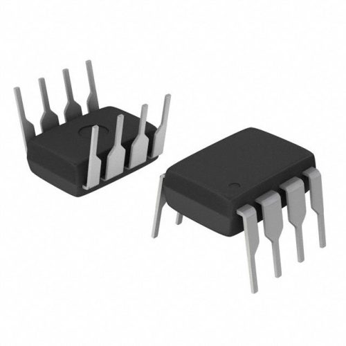
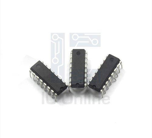
CD5313 Overview
The CD5313 is a CMOS integrated circuit designed to provide versatile digital logic functionality in industrial and electronic systems. It operates with low power consumption and features high noise immunity, making it suitable for a variety of logic applications. Its wide operating voltage range and robust design ensure reliable performance in harsh environments. This device is ideal for engineers and sourcing specialists seeking dependable components for complex digital logic implementations. For more detailed information and sourcing options, visit IC Manufacturer.
CD5313 Technical Specifications
| Parameter | Specification |
|---|---|
| Supply Voltage (VDD) | 3V to 15V |
| Input Voltage High (VIH) | ?? 0.7 ?? VDD |
| Input Voltage Low (VIL) | ?? 0.3 ?? VDD |
| Propagation Delay Time (tPLH, tPHL) | Typical 200 ns at VDD = 10V |
| Power Dissipation | Typically 10 ??W at VDD = 5V |
| Operating Temperature Range | -55??C to +125??C |
| Output Voltage High (VOH) | ?? VDD – 0.1V at IOH = -1.0 mA |
| Output Voltage Low (VOL) | ?? 0.1V at IOL = 1.0 mA |
CD5313 Key Features
- Wide Supply Voltage Range: Supports operation from 3V up to 15V, allowing flexible integration into various power environments without additional voltage regulation.
- Low Power Consumption: Utilizes CMOS technology for efficient operation, minimizing power dissipation to approximately 10 ??W at 5V, which is critical for energy-sensitive designs.
- High Noise Immunity: Ensures signal integrity in electrically noisy industrial settings, reducing false triggering and enhancing system reliability.
- Fast Propagation Delay: Typical delay times around 200 ns enable responsive digital logic operations, suitable for medium-speed logic circuits.
- Wide Operating Temperature Range: Functional from -55??C to +125??C, suitable for automotive, industrial, and harsh environmental applications.
CD5313 Advantages vs Typical Alternatives
This device offers superior integration with a wide voltage range and low power consumption compared to traditional TTL alternatives. Its CMOS design provides enhanced noise immunity and thermal stability, ensuring reliable performance in demanding industrial environments. The combination of fast switching times with low static current makes it an efficient and dependable choice for engineers seeking robust logic ICs.
🔥 Best-Selling Products
Typical Applications
- Digital logic control systems where reliable switching and low power are essential, such as in embedded industrial automation units requiring stable voltage tolerance and noise resistance.
- Interface logic circuits, facilitating communication between microprocessors and peripheral devices with varying voltage levels.
- Signal conditioning stages, improving signal integrity in environments with electrical interference.
- Custom logic function implementation in instrumentation and measurement equipment operating across wide temperature ranges.
CD5313 Brand Info
This integrated circuit is part of a well-established line of CMOS logic ICs known for their durability and precision. Manufactured with proven semiconductor processes, the device combines reliable performance with industry-standard pin configurations to simplify design and sourcing. It is widely recognized for meeting stringent industrial requirements, making it a preferred choice among engineers for critical digital logic applications.
FAQ
What supply voltage range does this device support?
The product supports a wide supply voltage range from 3V to 15V, allowing it to operate effectively in various power environments without compromising performance.
🌟 Featured Products
-

“Buy MAX9312ECJ+ Precision Voltage Comparator in DIP Package for Reliable Performance”
-
QCC-711-1-MQFN48C-TR-03-1 Bluetooth Audio SoC with MQFN48C Package
-

0339-671-TLM-E Model – High-Performance TLM-E Package for Enhanced Functionality
-
1-1415898-4 Connector Housing, Electrical Wire-to-Board, Receptacle, Packaged
How does the device perform in terms of power consumption?
Thanks to its CMOS technology, the device demonstrates low static power consumption, typically around 10 ??W at 5V supply, making it suitable for applications where energy efficiency is critical.
What is the typical propagation delay time, and why is it important?
The typical propagation delay is approximately 200 nanoseconds at 10V supply, enabling the device to handle medium-speed logic operations efficiently, which is important for timing-sensitive digital circuits.
📩 Contact Us
Can this component operate in extreme temperature conditions?
Yes, it supports an operating temperature range from -55??C to +125??C, ensuring reliable functionality in harsh industrial and automotive environments.
What are the output voltage characteristics under load?
Outputs maintain high voltage levels close to the supply voltage (at least VDD minus 0.1V at -1.0 mA) and low voltage levels near 0.1V at 1.0 mA load current, ensuring compatibility with standard logic input thresholds.

