CD5312 Overview
The CD5312 is a high-performance integrated circuit designed to deliver reliable and efficient digital logic functions in industrial and commercial applications. This device is known for its stable operation over a wide voltage range and robust switching capabilities, making it suitable for complex logic designs. Engineered to meet stringent quality standards, the CD5312 offers precise timing and logic control, enhancing overall system performance. Its compatibility with standard logic families ensures seamless integration into existing electronic systems. For more detailed information and sourcing, visit IC Manufacturer.
CD5312 Technical Specifications
| Parameter | Specification |
|---|---|
| Supply Voltage Range (VDD) | 3 V to 15 V |
| Input Voltage High (VIH) | Min 2.0 V at VDD = 5 V |
| Input Voltage Low (VIL) | Max 0.8 V at VDD = 5 V |
| Output Voltage High (VOH) | Min 3.5 V at VDD = 5 V, IO = -1.0 mA |
| Output Voltage Low (VOL) | Max 0.5 V at VDD = 5 V, IO = 1.6 mA |
| Input Current | ??1 ??A (typical) |
| Propagation Delay Time (tPD) | 25 ns (typical) at VDD = 10 V |
| Operating Temperature Range | -55??C to +125??C |
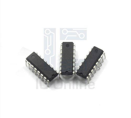
| Package Type | 16-pin Dual In-line Package (DIP) |
CD5312 Key Features
- Wide supply voltage range: Supports operation from 3 V to 15 V, enabling flexible design options and compatibility with various power sources.
- Low input current: Minimal input leakage current ensures high efficiency and reduces power consumption in complex circuits.
- Fast propagation delay: Typical delay of 25 ns allows for high-speed digital processing suitable for time-critical applications.
- High noise immunity: Robust input thresholds provide reliable performance in electrically noisy industrial environments.
- Wide operating temperature: Functional from -55??C to +125??C, making it ideal for harsh environments and automotive-grade applications.
- Standardized packaging: The 16-pin DIP format facilitates easy integration and replacement in existing designs.
CD5312 Advantages vs Typical Alternatives
The CD5312 stands out against typical logic IC alternatives due to its broad supply voltage tolerance, which enhances design flexibility. Its low input current reduces overall system power consumption, while fast switching speeds improve data throughput. The extended temperature range and high noise immunity ensure dependable operation in demanding industrial settings, making this device a reliable choice for engineers seeking robust and efficient logic components.
🔥 Best-Selling Products
Typical Applications
- Industrial control systems requiring precise logic control and reliable operation across varied power supplies and environmental conditions.
- Automotive electronics where wide temperature tolerance and noise immunity are critical for stable performance.
- Data processing units demanding fast switching and low power consumption to maximize efficiency.
- Embedded systems and digital signal processing circuits benefiting from standardized packaging and ease of integration.
CD5312 Brand Info
The CD5312 is a product within the CMOS digital logic family, produced by a reputable semiconductor manufacturer known for quality and consistency. This device aligns with industry standards for performance and reliability, ensuring compatibility with a wide range of applications. Its design emphasizes robustness and efficiency, supporting engineers and sourcing specialists in developing durable and high-performance electronic systems.
FAQ
What is the typical supply voltage range for the CD5312?
The device operates efficiently within a voltage range of 3 V to 15 V. This wide range allows it to be used in various power environments, from low-voltage battery systems to higher-voltage industrial power supplies.
🌟 Featured Products
-

“Buy MAX9312ECJ+ Precision Voltage Comparator in DIP Package for Reliable Performance”
-
QCC-711-1-MQFN48C-TR-03-1 Bluetooth Audio SoC with MQFN48C Package
-

0339-671-TLM-E Model – High-Performance TLM-E Package for Enhanced Functionality
-
1-1415898-4 Connector Housing, Electrical Wire-to-Board, Receptacle, Packaged
How does the CD5312 perform in terms of propagation delay?
It features a typical propagation delay of approximately 25 nanoseconds at a 10 V supply. This fast switching speed supports high-frequency digital circuits and time-sensitive applications.
What temperature conditions can the CD5312 withstand?
The component is rated to operate reliably in temperatures ranging from -55??C up to +125??C, making it suitable for automotive and harsh industrial environments where temperature extremes are common.
📩 Contact Us
What package type is used for the CD5312?
The device comes in a 16-pin Dual In-line Package (DIP), which is widely used and facilitates easy handling and installation on standard printed circuit boards.
How does the CD5312 manage power consumption?
With a typical input current of ??1 ??A, the device maintains very low power consumption during operation, which is beneficial for energy-sensitive applications and helps extend battery life in portable systems.

