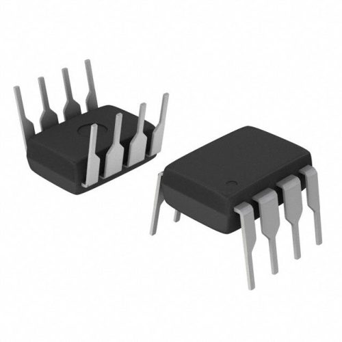
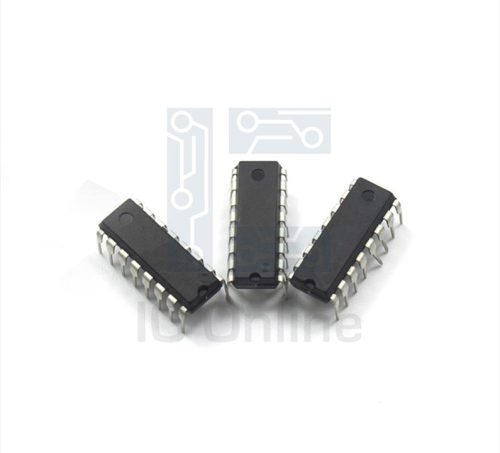
CD5310 Overview
The CD5310 is a high-performance integrated circuit designed for digital logic applications, offering reliable and efficient operation across a wide range of industrial environments. This device is optimized for use in complex digital systems requiring precise timing and control functions. With robust electrical characteristics and versatile input/output configurations, it supports seamless integration into various electronic designs. Engineers and sourcing specialists will appreciate its consistent performance and suitability for both standard and custom applications. For detailed product information and procurement, visit IC Manufacturer.
CD5310 Technical Specifications
| Parameter | Value | Unit |
|---|---|---|
| Supply Voltage Range | 3.0 to 15 | V |
| Input Voltage High (VIH) | 2.0 (min at VDD=5V) | V |
| Input Voltage Low (VIL) | 0.8 (max at VDD=5V) | V |
| Output Voltage High (VOH) | Min 3.5 (at IOH = -0.4mA) | V |
| Output Voltage Low (VOL) | Max 0.5 (at IOL = 4.0mA) | V |
| Propagation Delay Time | 50 | ns |
| Operating Temperature Range | -55 to 125 | ??C |
| Power Dissipation | 500 | mW |
CD5310 Key Features
- Wide Supply Voltage Range: Supports operation from 3.0 V up to 15 V, enabling flexibility in system design and compatibility with various power domains.
- Fast Propagation Delay: Typical delay time of 50 ns ensures rapid signal processing, which is critical for timing-sensitive digital circuits.
- Robust Input Thresholds: Defined VIH and VIL levels guarantee noise immunity and signal integrity in noisy industrial environments.
- Low Power Dissipation: With a maximum dissipation of 500 mW, it supports energy-efficient designs that contribute to extended system lifetime.
CD5310 Advantages vs Typical Alternatives
This device offers superior voltage tolerance and fast switching speed compared to many standard digital ICs. Its wide supply voltage range and low power consumption make it ideal for applications where energy efficiency and reliable performance are critical. Additionally, the clearly specified input and output voltage thresholds enhance noise immunity and integration ease, setting it apart from less robust alternatives.
🔥 Best-Selling Products
Typical Applications
- Digital timing and control circuits in industrial automation systems, where accurate signal processing and reliable operation under varied voltage levels are essential.
- Logic interface modules requiring compatibility with multiple logic families and power supply configurations.
- Embedded system controllers that need fast response times and stable digital signals for precise operation.
- Signal conditioning blocks in communication equipment, benefiting from low propagation delay and defined voltage thresholds.
CD5310 Brand Info
The CD5310 is manufactured under the reputed IC Manufacturer brand, known for delivering high-quality semiconductor solutions tailored to industrial and commercial electronics markets. This product line emphasizes precision, robustness, and ease of integration, supporting engineers worldwide in developing reliable digital systems. The CD5310 continues this tradition by offering a dependable logic device designed to meet stringent performance and environmental requirements.
FAQ
What supply voltage range does the CD5310 support?
The device operates across a wide supply voltage range from 3.0 V to 15 V, allowing it to be used in various power environments and providing flexibility for different system designs.
🌟 Featured Products
-

“Buy MAX9312ECJ+ Precision Voltage Comparator in DIP Package for Reliable Performance”
-
QCC-711-1-MQFN48C-TR-03-1 Bluetooth Audio SoC with MQFN48C Package
-

0339-671-TLM-E Model – High-Performance TLM-E Package for Enhanced Functionality
-
1-1415898-4 Connector Housing, Electrical Wire-to-Board, Receptacle, Packaged
How fast is the propagation delay of this IC?
The typical propagation delay time is approximately 50 nanoseconds, enabling rapid signal transitions suitable for timing-critical applications in digital circuits.
What are the input voltage thresholds for logic high and low levels?
At a supply voltage of 5 V, the minimum input voltage recognized as a logical high (VIH) is 2.0 V, while the maximum voltage for a logical low (VIL) is 0.8 V, ensuring reliable logic level discrimination.
📩 Contact Us
Can this device operate reliably in extreme temperature conditions?
Yes, it supports an operating temperature range from -55??C to 125??C, making it suitable for harsh industrial environments and outdoor applications.
What is the typical power dissipation of the device?
The maximum power dissipation is specified at 500 milliwatts, allowing for efficient thermal management in compact electronic designs and contributing to overall system reliability.

