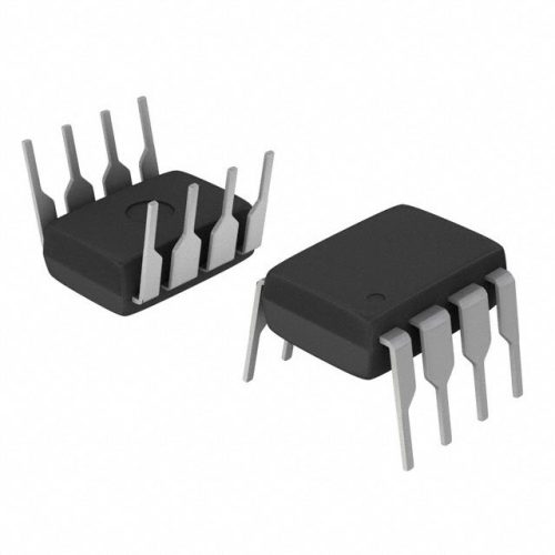
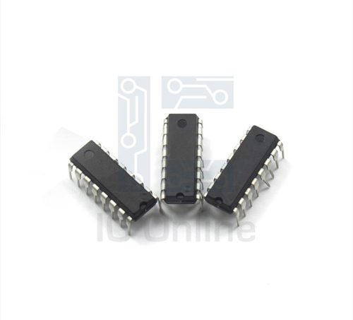
CD5298 Overview
The CD5298 is a versatile CMOS integrated circuit designed for electronic applications requiring precision and reliable logic control. This device operates efficiently under a wide voltage range, making it suitable for diverse industrial and commercial environments. Its robust design ensures consistent performance in complex digital systems. Engineers and sourcing specialists value the CD5298 for its stable switching characteristics and compatibility with various digital logic families, enhancing system integration and reducing design complexity. For detailed technical specifications and additional product information, visit IC Manufacturer.
CD5298 Technical Specifications
| Parameter | Value |
|---|---|
| Supply Voltage (VDD) | 3 V to 15 V |
| Input Voltage Range | 0 to VDD |
| Operating Temperature Range | -55??C to +125??C |
| Propagation Delay Time | Typical 70 ns at 10 V |
| Quiescent Supply Current | 1 ??A typical at 5 V |
| Output Drive Current | ??10 mA |
| Logic Family | CMOS |
| Package Type | 14-pin Dual In-line Package (DIP) |
CD5298 Key Features
- Wide Operating Voltage Range: Supports 3 V to 15 V supply voltages, allowing flexible integration into various power environments.
- Low Power Consumption: Typical quiescent current of 1 ??A reduces power dissipation, ideal for battery-powered or energy-sensitive applications.
- High Noise Immunity: CMOS design ensures strong noise margins, improving reliability in electrically noisy industrial conditions.
- Fast Switching Speed: Propagation delay as low as 70 ns enables efficient high-frequency digital signal processing.
CD5298 Advantages vs Typical Alternatives
Compared to traditional TTL logic devices, this product offers significant advantages in power efficiency and voltage flexibility. Its CMOS technology provides higher noise immunity and lower static power consumption. Additionally, the wide supply voltage range and fast switching capability deliver improved integration potential and operational reliability in demanding industrial and commercial digital circuits.
🔥 Best-Selling Products
Typical Applications
- Digital logic signal interfacing in industrial control systems where wide voltage tolerance and low power operation are critical.
- Battery-powered electronic devices requiring minimal quiescent current to extend operational life.
- Noise-sensitive environments needing robust logic components with high noise margins for signal integrity.
- General-purpose logic circuitry in embedded systems and microcontroller interfaces.
CD5298 Brand Info
The CD5298 is part of a well-established line of CMOS logic devices offered by the manufacturer, known for delivering reliable and high-performance integrated circuits to the electronics industry. This product exemplifies the brand??s commitment to quality, innovation, and broad applicability across industrial and commercial markets. Its design focuses on meeting rigorous performance and reliability standards, ensuring seamless integration into complex electronic systems.
FAQ
What supply voltage range does this device support?
This integrated circuit operates over a broad supply voltage range from 3 V up to 15 V, making it compatible with both low-voltage digital systems and higher-voltage industrial power supplies.
🌟 Featured Products
-

“Buy MAX9312ECJ+ Precision Voltage Comparator in DIP Package for Reliable Performance”
-
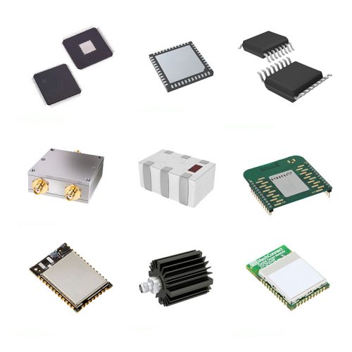
QCC-711-1-MQFN48C-TR-03-1 Bluetooth Audio SoC with MQFN48C Package
-

0339-671-TLM-E Model – High-Performance TLM-E Package for Enhanced Functionality
-
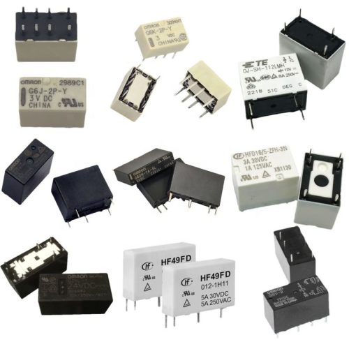
1-1415898-4 Connector Housing, Electrical Wire-to-Board, Receptacle, Packaged
How does the power consumption of this device compare to other logic ICs?
The device features a very low quiescent supply current, typically around 1 ??A at 5 V, which is significantly lower than many TTL counterparts, enhancing energy efficiency especially in battery-operated applications.
What package types are available for this product?
It is available in a 14-pin Dual In-line Package (DIP), which is widely used for easy prototyping, testing, and integration into through-hole circuit boards.
📩 Contact Us
Can this device operate reliably in harsh temperature environments?
Yes, it is rated for operation from -55??C up to +125??C, ensuring dependable performance in a variety of industrial and outdoor applications where temperature extremes are common.
What are the typical use cases for this component?
Typical applications include digital logic interfacing in industrial controls, battery-powered electronics, noise-sensitive environments, and general-purpose embedded systems requiring stable and efficient logic operations.

