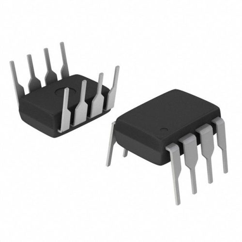
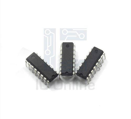
CD5296 Overview
The CD5296 is a versatile integrated circuit designed for efficient digital logic applications requiring reliable high-voltage switching and signal processing. It features complementary MOS technology optimized for robust operation in industrial environments. With a wide supply voltage range and low quiescent current, this device is suited for systems where power efficiency and operational stability are critical. Its construction ensures compatibility with standard logic levels, making it ideal for interfacing and driving various loads. Engineers and sourcing specialists can rely on this solution for consistent performance in control and switching circuits. For more technical support and product options, visit IC Manufacturer.
CD5296 Technical Specifications
| Parameter | Specification |
|---|---|
| Supply Voltage (VDD) | 3 V to 15 V |
| Input Voltage Range | 0 V to VDD |
| Maximum Input Current | ??1 ??A (typical) |
| Propagation Delay Time | Typical 50 ns |
| Output Current | ??10 mA (max) |
| Operating Temperature Range | -55??C to +125??C |
| Power Dissipation | 500 mW (max) |
| Input Threshold Voltage | Approximately 1.5 V at VDD = 5 V |
| Package Type | 16-pin Dual In-line Package (DIP) |
CD5296 Key Features
- Wide supply voltage range: Operates reliably from 3 V to 15 V, allowing flexible integration into various power domains.
- Low input current: Inputs draw minimal current (typical ??1 ??A), reducing power consumption and minimizing load on preceding stages.
- Fast switching speed: Typical propagation delay of 50 ns ensures efficient signal processing in high-speed digital circuits.
- High output drive capability: Capable of sourcing and sinking up to ??10 mA, suitable for driving LEDs, relays, or other moderate loads directly.
- Wide operating temperature range: Designed for industrial environments with operation guaranteed between -55??C and +125??C.
- Standard logic compatibility: Input thresholds compatible with TTL and CMOS logic levels, simplifying system design and interfacing.
- Robust packaging: Available in a 16-pin DIP package, compatible with through-hole mounting and prototyping environments.
CD5296 Advantages vs Typical Alternatives
This device offers advantages such as a broad supply voltage range and low input current compared to typical alternatives. Its high output drive capability improves integration efficiency by reducing the need for additional buffering components. The fast switching speeds contribute to improved system responsiveness. Additionally, its wide temperature tolerance and robust packaging enhance reliability in demanding industrial applications, making it a preferred choice for engineers seeking durable and efficient digital logic solutions.
🔥 Best-Selling Products
Typical Applications
- Logic level shifting and buffering in industrial control systems, enabling reliable interface between various voltage domains and signal types.
- Driving indicator LEDs and status displays directly, leveraging its output current capability for simple visual feedback circuits.
- Signal conditioning and processing in embedded systems requiring stable and fast digital logic operations under varied environmental conditions.
- Relay driver circuits where moderate current sourcing and sinking are required to actuate electromechanical switches safely and efficiently.
CD5296 Brand Info
The CD5296 is part of a well-established series of CMOS logic devices known for their robustness and versatility in industrial electronics. This product line emphasizes broad operating voltage and temperature ranges, catering to demanding environments. The manufacturer’s commitment to high-quality semiconductor design ensures consistent performance and reliability, making this device a trusted component for engineers and sourcing professionals focusing on long-term system stability and efficiency.
FAQ
What is the typical supply voltage range for this device?
The device operates effectively within a supply voltage range of 3 V to 15 V, offering flexibility for integration across low-voltage and higher-voltage digital systems.
🌟 Featured Products
-

“Buy MAX9312ECJ+ Precision Voltage Comparator in DIP Package for Reliable Performance”
-
QCC-711-1-MQFN48C-TR-03-1 Bluetooth Audio SoC with MQFN48C Package
-

0339-671-TLM-E Model – High-Performance TLM-E Package for Enhanced Functionality
-
1-1415898-4 Connector Housing, Electrical Wire-to-Board, Receptacle, Packaged
How does the device handle input current requirements?
Inputs draw very low current, typically around ??1 ??A, which minimizes power consumption and reduces the electrical load on preceding circuit stages, enhancing overall system efficiency.
Can this component drive moderate loads directly?
Yes, it can source and sink output currents up to ??10 mA, making it suitable for directly driving LEDs, relays, and other moderate loads without needing additional driver circuits.
📩 Contact Us
What temperature range can the device reliably operate within?
It supports an operating temperature range from -55??C to +125??C, allowing reliable use in industrial and harsh environmental conditions where temperature extremes are common.
Is the device compatible with standard logic families?
Yes, the input threshold voltages are designed to be compatible with both TTL and CMOS logic levels. This compatibility simplifies interfacing with a wide range of digital circuits and systems.

