2N4959UB/TR Overview
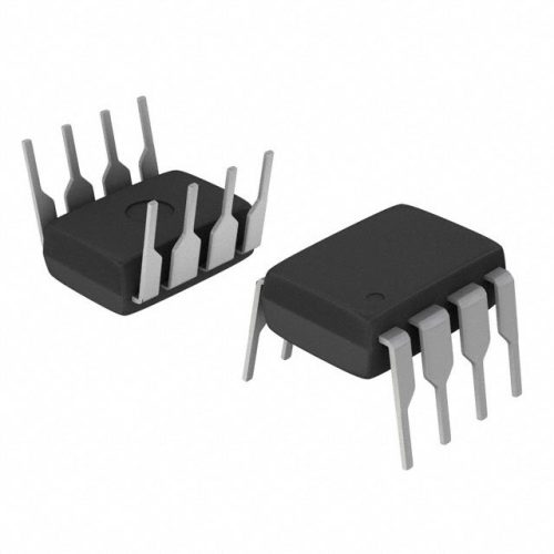
The 2N4959UB/TR is a high-performance N-channel JFET transistor designed for precision analog switching and low-noise amplification in industrial electronics. Offering robust electrical characteristics and stable operation, this transistor supports applications requiring reliable switching and signal integrity. Available in a through-hole package, it facilitates easy integration into various circuit designs. Engineers and sourcing specialists benefit from its consistent parameters, making it a dependable choice for signal processing and amplification in demanding environments. For more detailed technical insights, visit the IC Manufacturer website.
2N4959UB/TR Key Features
- Low Noise Performance: Enables high-fidelity signal amplification, critical for sensitive measurement and audio applications.
- High Input Impedance: Minimizes loading on preceding stages, preserving signal integrity in precision circuits.
- Stable Electrical Characteristics: Ensures consistent switching behavior and reliability under varying operational conditions.
- Robust Package Design: The through-hole form factor allows for durable mechanical mounting and easy prototyping or repair.
2N4959UB/TR Technical Specifications
| Parameter | Specification |
|---|---|
| Type | N-Channel JFET |
| Drain-Source Voltage (VDS) | 30 V |
| Gate-Source Cutoff Voltage (VGS(off)) | -0.3 to -6 V |
| Drain Current (ID) | 10 mA (max) |
| Power Dissipation (PD) | 400 mW |
| Input Capacitance (Ciss) | 3 pF (typical) |
| Noise Figure | 2 dB (typical) |
| Operating Temperature Range | -55??C to +150??C |
2N4959UB/TR Advantages vs Typical Alternatives
This transistor provides superior low-noise operation and higher input impedance compared to typical alternatives, enhancing signal clarity and reducing distortion in sensitive analog circuits. Its robust voltage and current ratings, combined with a stable operating temperature range, make it a reliable component for industrial switching and amplification tasks. The through-hole package also offers easier handling and replacement compared to surface-mount counterparts, facilitating maintenance and prototyping.
🔥 Best-Selling Products
Typical Applications
- Precision low-noise amplifiers in sensor signal conditioning, where maintaining signal integrity is essential to accurate measurement.
- Analog switching circuits requiring fast, reliable gate control with minimal signal loss.
- Audio preamplifier stages that benefit from low noise and high input impedance characteristics.
- Industrial instrumentation systems demanding durable, stable transistors for extended operational lifetimes.
2N4959UB/TR Brand Info
The 2N4959UB/TR is a well-established product in the semiconductor portfolio, known for its consistent quality and performance in analog switching applications. Manufactured under stringent quality controls, it meets industrial standards for reliability and electrical performance. This device is frequently selected by engineers for its proven track record in precision circuits and robust package design, backed by comprehensive datasheet support and manufacturer availability.
FAQ
What is the typical application environment for this transistor?
The transistor is commonly used in environments requiring stable analog switching and low-noise amplification, such as industrial instrumentation and audio signal processing. Its broad operating temperature range supports use in harsh or variable conditions.
🌟 Featured Products
-

“Buy MAX9312ECJ+ Precision Voltage Comparator in DIP Package for Reliable Performance”
-

QCC-711-1-MQFN48C-TR-03-1 Bluetooth Audio SoC with MQFN48C Package
-

0339-671-TLM-E Model – High-Performance TLM-E Package for Enhanced Functionality
-

1-1415898-4 Connector Housing, Electrical Wire-to-Board, Receptacle, Packaged
How does the gate-source cutoff voltage affect circuit design?
The gate-source cutoff voltage defines the voltage level at which the transistor switches off. Designers use this parameter to ensure proper biasing and switching thresholds, which are critical for achieving precise control in analog switching and amplification circuits.
Can this transistor handle high power dissipation?
The device supports power dissipation up to 400 mW, suitable for moderate power applications. Proper heat management, such as heat sinking or PCB thermal design, should be considered to maintain reliability within the specified ratings.
📩 Contact Us
Is the through-hole package beneficial for prototyping?
Yes, the through-hole package facilitates easy insertion and removal on standard prototyping boards, making it ideal for testing and development phases. It also provides mechanical stability in final product assemblies requiring robust mounting.
What are the noise performance characteristics of this transistor?
This transistor exhibits a typical noise figure of 2 dB, indicating low noise generation during signal amplification. This characteristic is important in applications where signal clarity and minimal distortion are priorities, such as audio and sensor interfaces.


