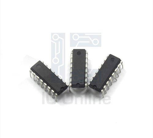
JANKCB2N5002-Transistor-Die Overview
The JANKCB2N5002-Transistor-Die is a high-performance semiconductor component designed for precise switching and amplification applications. Engineered for optimal electrical characteristics, this transistor die offers reliable operation under various industrial conditions. Its compact die form factor supports integration into custom packaging and allows for efficient thermal management. Ideal for engineers and sourcing specialists, this device ensures consistent performance in power control circuits and signal modulation. For more detailed product sourcing and technical support, visit Fabricante de CI.
JANKCB2N5002-Transistor-Die Technical Specifications
| Parámetro | Especificación |
|---|---|
| Tipo | NPN Bipolar Junction Transistor (BJT) |
| Tensión colector-emisor (VDIRECTOR GENERAL) | 500 V |
| Corriente de colector (IC) | 2 A |
| Disipación de potencia (PD) | 30 W |
| Frecuencia de transición (fT) | 100 MHz |
| Ganancia Ancho de banda Producto | 100 MHz |
| Tipo de envase | Transistor Die (Bare Die) |
| Temperatura de funcionamiento | -55 ??C to +150 ??C |
| Tensión base del emisor (VBE) | 1.2 V typical |
JANKCB2N5002-Transistor-Die Key Features
- Capacidad de alta tensión: Supports up to 500 V collector-emitter voltage, enabling use in high-voltage power applications.
- Robust current handling: Rated for 2 A collector current, suitable for medium power amplification and switching tasks.
- Compact die form: Bare die format allows for custom packaging and thermal optimization in demanding industrial environments.
- Amplia gama de temperaturas de funcionamiento: Reliable performance from -55 ??C to +150 ??C ensures stability in harsh conditions.
- High transition frequency: 100 MHz frequency response supports fast switching and high-speed signal processing.
Aplicaciones típicas
- Industrial power supply circuits where high voltage and current switching is required, such as motor drivers and voltage regulators.
- Signal amplification stages in communication equipment demanding high gain and frequency response.
- Custom semiconductor module integration requiring a bare die for embedding into specialized packages.
- Automotive electronic control units that operate under wide temperature ranges and require robust transistor performance.
JANKCB2N5002-Transistor-Die Advantages vs Typical Alternatives
This transistor die offers superior voltage and current ratings compared to typical discrete transistors, enabling more robust power handling in compact form factors. Its bare die format provides flexibility for custom packaging, improving thermal management and integration in specialized industrial applications. The wide operating temperature range and high transition frequency also contribute to enhanced reliability and performance in demanding electronic environments.
Productos más vendidos
-
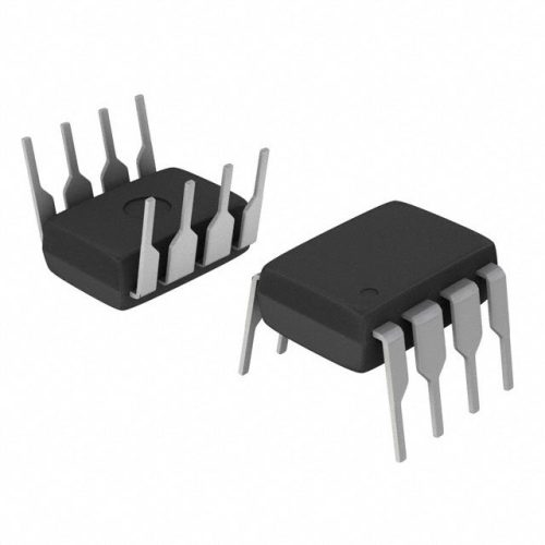
TLC555 Timer IC - Temporizador de precisión de Texas Instruments en encapsulado PDIP-8
-

Texas Instruments TL081 Op Amp de entrada JFET de bajo ruido - encapsulado DIP-8
-

Texas Instruments UC3842 Controlador PWM de modo de corriente - Paquete DIP-8
-

Texas Instruments LM2937 Regulador de voltaje encapsulado TO-220 - Lineal de baja caída
JANKCB2N5002-Transistor-Die Brand Info
The JANKCB2N5002 transistor die is manufactured by a leading semiconductor producer specializing in high-voltage bipolar transistors for industrial and automotive markets. This product reflects the brand??s commitment to quality, reliability, and innovation in transistor technology. Their portfolio includes a wide range of transistor dies optimized for power applications, ensuring customers can select components tailored to stringent technical requirements and harsh operating conditions. The company supports extensive technical documentation and customer service for seamless integration into complex systems.
PREGUNTAS FRECUENTES
What is the maximum collector-emitter voltage of this transistor die?
The maximum collector-emitter voltage rating is 500 volts, making it suitable for high-voltage switching and amplification applications in industrial circuits.
Productos destacados
-

"Compre el comparador de tensión de precisión MAX9312ECJ+ en encapsulado DIP para un rendimiento fiable"
-
QCC-711-1-MQFN48C-TR-03-1 Bluetooth Audio SoC with MQFN48C Package
-

Modelo 0339-671-TLM-E - Paquete TLM-E de alto rendimiento para una funcionalidad mejorada
-
1-1415898-4 Carcasa del conector, cable eléctrico a placa, receptáculo, empaquetado
Can this transistor die handle continuous high current loads?
Yes, it is rated for a collector current of up to 2 amperes, allowing it to manage continuous medium power loads effectively within its thermal limits.
What is the significance of the transistor die format for application engineers?
The bare die format allows engineers to integrate the transistor directly into custom packages or modules, providing enhanced thermal conductivity and enabling compact design solutions tailored to specific industrial needs.


