
What Is Input Overvoltage Protection?
Input overvoltage protection (OVP) is one of those design elements that rarely gets praise when it works—and causes chaos when it doesn’t. It sits quietly at the front end of an electronic system, absorbing abuse, blocking mistakes, and protecting value. From consumer gadgets to industrial controllers, input OVP is the difference between resilience and regret.
Short sentence. Big impact.
This article explains what input overvoltage protection is, why it matters, how it works, and how to design it correctly, using plain language while keeping technical depth. The goal is practical understanding—not theory for theory’s sake.
1. Definition and Scope of Input Overvoltage Protection
Input overvoltage protection is a design technique that prevents excessive voltage at a system’s input from damaging downstream circuits.
“Input” means the very first electrical interface:
- DC inputs (adapters, batteries, PoE rails)
- AC mains (line and neutral)
- Signal and communication lines
Overvoltage occurs when the applied voltage exceeds the maximum safe operating limit—either briefly (microseconds) or for long durations (seconds or more).
Input OVP vs Output OVP
| Aspect | Input OVP | Output OVP |
|---|---|---|
| Protection focus | Incoming power or signal | Regulated output rail |
| Primary threat | External sources | Internal control failure |
| Typical location | Connector / power entry | Inside regulator loop |
| Failure impact | System-wide damage | Load-side damage |
Input OVP protects the entire system. Output OVP protects what you power. Confusing the two is a costly mistake.
2. Why Input Overvoltage Protection Matters
Overvoltage damage is rarely gentle.
A single event can:
- Punch through MOSFET gates
- Dry out electrolytic capacitors
- Trigger latent failures that appear months later
Engineering and Business Risks
| Without Proper OVP | With Proper OVP |
|---|---|
| Burned components | Graceful shutdown |
| Intermittent field failures | Predictable behavior |
| High RMA rates | Lower warranty cost |
| Certification failures | Faster approvals |
From a lifecycle view, the cost of prevention is trivial compared to the cost of failure.
As reliability expert Fred Schindler famously said:
“If you don’t design for abuse, the real world will do it for you.”
3. Types and Causes of Input Overvoltage Events
Not all overvoltage events are equal.
Common Overvoltage Categories
- Transient spikes (nanoseconds to microseconds)
- Sustained overvoltage (seconds or longer)
- AC overvoltage (mains surges)
- DC overvoltage (wrong adapters, load dump)
Real-World Causes
- Incorrect or cheap power adapters
- Automotive load dump events
- Hot-plugging long cables
- Inductive switching in industrial systems
- Grid disturbances and PSU failures
Industry standards such as those from IEC define test waveforms—but reality is often worse.
4. How Input Overvoltage Protection Works
All OVP circuits follow the same basic logic:
- Monitor voltage
- Detect threshold violation
- Respond fast
- Handle energy safely
Response Mechanisms
| Method | Behavior | Risk |
|---|---|---|
| Clamping | Limits voltage | High power dissipation |
| Disconnect | Opens circuit | Needs fast detection |
| Crowbar | Shorts input | Blows fuse |

The right response depends on voltage level, duration, and energy—not just peak value.
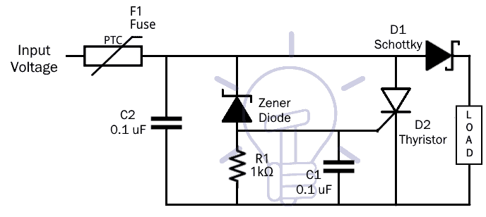
5. Common Input Overvoltage Protection Methods
Designers can choose from discrete parts, integrated ICs, or hybrids.
Popular Techniques
| Method | Strength | Limitation |
|---|---|---|
| TVS / Zener | Fast, simple | Heat stress |
| SCR crowbar | Rugged | System shutdown |
| MOSFET disconnect | Efficient | Design complexity |
| eFuse / OVP IC | Compact | Cost |
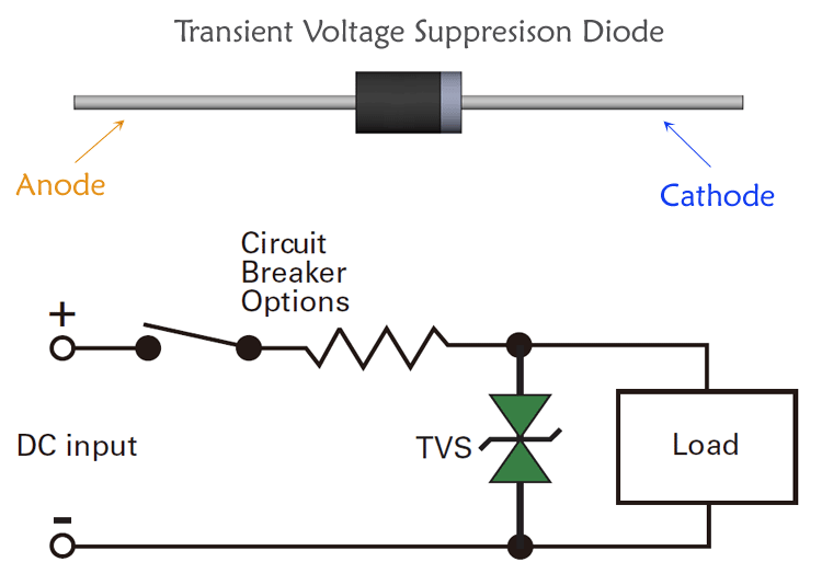


Modern designs often use hybrid architectures—for example, a TVS diode for fast spikes and a MOSFET-based OVP IC for sustained faults.
6. Discrete vs Integrated OVP Solutions
Choosing between discrete and integrated solutions is a trade-off, not a rule.
Comparison Overview
| Factor | Discrete Design | Integrated IC |
|---|---|---|
| BOM count | High | Low |
| PCB area | Larger | Smaller |
| Threshold accuracy | Depends on parts | Factory-trimmed |
| Design effort | High | Low |
| Long-term reliability | Variable | Consistent |
Integrated solutions shine in consumer and compact designs. Discrete circuits remain common in high-voltage or harsh environments.
7. Key Design Parameters That Matter
OVP design fails when details are ignored.
Critical Electrical Parameters
- Threshold accuracy: Too close to nominal = nuisance trips
- Response time: ns for ESD, µs for surges, ms for sustained faults
- Clamping voltage: Must stay below absolute max ratings
- Thermal limits: TVS power ratings are not suggestions
- Leakage current: Impacts efficiency and standby power
Good designers leave margin. Great designers document why.
8. Input Overvoltage Protection Across Applications
Context changes everything.
| Application | Key OVP Concern |
|---|---|
| Consumer electronics | Wrong adapters |
| Automotive | Load dump, cold crank |
| Industrial | Inductive transients |
| Telecom | Lightning-induced surges |
| Medical | Safety and isolation |
In medical and safety-critical systems, input OVP is not optional. It directly affects compliance, patient safety, and liability.
Final Thoughts on Designing with Input Overvoltage Protection
Input overvoltage protection is not a feature.
It is infrastructure.
When designed early, it:
- Prevents catastrophic failures
- Improves certification success
- Reduces warranty cost
- Extends product life
When ignored, it becomes an expensive lesson.
Smart teams treat input OVP as a strategic design decision, not a last-minute patch. IC manufacturers, protection standards, and modern tools make robust solutions easier than ever.
Design for the real world.
Because the real world will test you—eventually.
