
What Is ESD Protection in ICs?
Electrostatic Discharge (ESD) protection is one of the least visible yet most critical design elements in modern integrated circuits (ICs).
It does not improve speed.
It does not add features.
But without it, even the most advanced chip can fail before it ever reaches the customer.
As an old engineering proverb often attributed to reliability experts goes:
“A circuit that works in the lab but fails in the field is not a finished design.”
This article explains what ESD protection is, how it works inside ICs, why it matters for reliability and cost, and how engineers should evaluate it—all at a clear, practical, 7th-grade reading level.
1. Understanding ESD in Integrated Circuits
Electrostatic Discharge is the sudden flow of electricity between two objects with different electrical potentials. In daily life, it feels like a small shock. Inside an IC, it can be catastrophic.
Modern chips operate at less than 1 volt.
ESD events can reach thousands of volts—even when humans cannot feel them.
What Electrostatic Discharge Really Means
In ICs, ESD is a high-current, ultra-fast pulse. It lasts nanoseconds, but the current can exceed several amperes. That is enough to melt silicon or rupture ultra-thin oxides.
Common Scenarios Where ESD Occurs
- Human handling during assembly
- Automated pick-and-place tools
- Wafer probing and package testing
- PCB insertion and connector mating
Why Low-Voltage ESD Still Destroys ICs
Advanced CMOS gate oxides are only a few atomic layers thick.
They are fast—but fragile.
ESD vs. EOS (Electrical Overstress)
ESD is fast and sharp.
EOS is slower and sustained.
They cause different failure signatures, but both can silently kill reliability.
2. Why ESD Protection Is Critical for IC Reliability
ESD does not always cause instant failure.
That is what makes it dangerous.
Early-Life Failures
Unprotected ICs may fail during first power-up. This is called infant mortality.
Latent Damage
Some ESD events weaken a device without killing it.
Months later, it fails in the field.
Business Impact
- Higher RMA rates
- Qualification delays
- Brand damage
- Lost customers
In high-volume electronics, one weak ESD design can cost millions.
3. How ESD Protection Works Inside an IC
ESD protection structures act like emergency exits for current.
They stay invisible during normal operation.
They activate only during an ESD strike.


Purpose of On-Chip ESD Protection
- Detect abnormal voltage spikes
- Turn on quickly
- Safely shunt current to ground
Diverting ESD Away from Core Circuits
Without protection, ESD flows through logic gates.
With protection, current flows through designed sacrificial paths.
Pad Rings and Power Clamps
Most ESD devices sit near I/O pads and power rails, forming a defensive ring around sensitive logic.
4. Common On-Chip ESD Protection Structures
Not all ESD protection looks the same. Different ICs need different strategies.


Diode-Based Protection
- Simple
- Fast
- Low cost
Often used in basic logic and analog ICs.
ESD Clamps
Active devices that turn on only during ESD events.
Essential for advanced nodes and low-voltage cores.
Resistor and MOS-Based Devices
Used to slow current rise and distribute energy safely.
5. Key ESD Design Parameters and Trade-Offs
Every ESD design is a compromise.
Trigger Voltage and Holding Voltage
Too high → protection activates too late.
Too low → false triggering.
Response Time
ESD events rise in sub-nanoseconds.
Protection must react faster than logic gates.
Leakage vs. Reliability
Stronger protection increases leakage and die area.
Signal Integrity Impact
High-speed interfaces suffer from added capacitance.
| Interface Type | ESD Challenge | Design Trade-Off |
|---|---|---|
| USB / HDMI | High data rate | Low capacitance |
| RF | Noise sensitivity | Minimal parasitics |
| SerDes | Timing margin | Balanced clamp strength |
6. ESD Standards, Models, and Compliance
ESD protection is not guesswork.
It is measured against global standards.

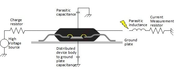
IC-Level ESD Models
- HBM (Human Body Model)
- CDM (Charged Device Model)
- MM (largely obsolete)
Standards Organizations
- JEDEC defines IC qualification rules
- IEC governs system-level tests
Why IC Ratings ≠ System Robustness
A 2 kV HBM IC can still fail a system-level IEC test.
Board design and external protection matter.
7. IC-Level vs. System-Level ESD Protection
On-chip ESD is necessary but not sufficient.
What IC-Level Protection Can Do
- Survive handling and assembly
- Protect internal logic
What It Cannot Do
- Absorb repeated IEC gun strikes
- Protect long external cables
When External Protection Is Mandatory
- Automotive electronics
- Industrial controls
- I/O-heavy consumer devices
| Application | External ESD Needed |
|---|---|
| Automotive ECU | Always |
| USB Devices | Usually |
| Simple MCU Board | Sometimes |
8. Manufacturing, Handling, and Lifecycle Considerations
Even the best ESD design fails if handling is careless.
Manufacturing Risks
- Wafer probing
- Package assembly
- Automated test equipment
ESD-Safe Handling
- Grounded workstations
- ESD bags and trays
- Controlled EPA zones
Testing and Qualification
ESD validation happens before and after silicon.
Correlation with field data is essential—but never perfect.
Key Takeaways
- ESD protection is foundational, not optional
- Advanced nodes are faster—but weaker
- On-chip protection must be co-designed with system protection
- Standards guide testing, not real-world guarantees
- Reliability begins long before the product ships
In IC design, speed wins benchmarks.
Reliability wins markets.
