


Semiconductor Doping Basics for ICs: A Practical Guide for Engineers, Decision-Makers, and Supply Chain Leaders
Semiconductor doping is invisible to the naked eye—yet it defines everything. Speed or slowness. Yield or scrap. Reliability or recall. In modern integrated circuits (ICs), doping is not a background process. It is the foundation.
This guide strips away theory-heavy jargon and replaces it with practical insight. Engineers will see the physics clearly. Executives will understand the cost and risk implications. Supply chain leaders will recognize why doping transparency matters more than datasheets suggest.
Introduction to Semiconductor Doping
Semiconductor doping is the intentional introduction of impurity atoms into pure silicon to control its electrical behavior. Pure silicon, by itself, is nearly useless for logic. It conducts poorly. It switches slowly. It cannot form functional transistors at scale.
By adding carefully chosen dopant atoms—often at concentrations of only one part per million—engineers transform silicon into a controllable electrical material. This tiny change unlocks massive capability.
In ICs, doping determines:
- Whether current flows easily or reluctantly
- Where junctions form
- How fast transistors switch
- How much power leaks when they should be off
A common proverb in manufacturing applies perfectly here: “What you don’t control will control you.” In semiconductor fabrication, doping control is that truth made physical.
Why Doping Is Critical for Integrated Circuits
Every transistor in an IC depends on doping. Without it, there is no on-state, no off-state, and no logic.
Doping defines:
- Source and drain conductivity
- Channel threshold voltage
- Junction depth and leakage
- Device isolation
Poor doping control leads to hard failures—shorts, opens, excessive leakage. Worse, it causes soft failures: marginal timing, unstable thresholds, early aging. These are the failures that escape testing and return as field defects.
From a business standpoint, the consequences are stark:
| Impact Area | Poor Doping Control Leads To |
|---|---|
| Yield | Parametric fallout, bin loss |
| Cost | Rework, scrap, lower margins |
| Reliability | Early-life and latent failures |
| Time-to-market | Debug cycles and qualification delays |
In short: doping precision is not an engineering luxury. It is a competitive necessity.
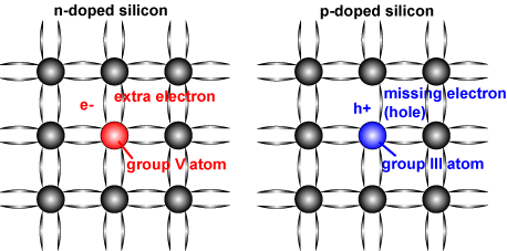
N-Type and P-Type Semiconductors
Doping creates two fundamental semiconductor types: N-type and P-type. Their interaction is the basis of all IC functionality.
- N-type silicon is doped with donor atoms (like phosphorus). These atoms contribute extra electrons, making electron conduction dominant.
- P-type silicon is doped with acceptor atoms (like boron). These create “holes,” which act as positive charge carriers.
Neither is better. Both are essential.
Their applications differ:
| Doping Type | Majority Carrier | Typical IC Use |
|---|---|---|
| N-type | Electrons | NMOS source/drain, wells |
| P-type | Holes | PMOS source/drain, wells |
Modern CMOS technology relies on precise symmetry between these two worlds. When balance breaks, performance collapses.
Common Dopant Materials Used in IC Manufacturing
Only a handful of elements are suitable as dopants. The reasons are strict: atomic size, solubility, diffusion behavior, and electrical stability.
Common N-type dopants
- Phosphorus
- Arsenic
- Antimony
Common P-type dopants
- Boron
- Gallium (less common, niche applications)
Selection is never arbitrary. Engineers evaluate:
- Lattice compatibility – mismatch causes defects
- Diffusion rate – affects junction depth
- Activation energy – impacts thermal budgets
- Reliability – resistance to clustering and deactivation
A famous engineering maxim applies here: “The cheapest choice is often the most expensive in hindsight.” Dopant selection proves it repeatedly.
PN Junctions and Doping Profiles
When N-type and P-type regions meet, a PN junction forms. This junction is the heart of diodes, transistors, and IC logic.
But junctions are not binary. Their behavior depends on doping profiles:
- Uniform profiles: simple, predictable, but limited
- Graded profiles: smoother electric fields, better control
- Shallow junctions: faster switching, higher leakage risk
- Deep junctions: robust, slower, more power-hungry
These trade-offs directly affect:
- Threshold voltage
- Short-channel effects
- Leakage current
- Device scalability
At advanced nodes, even nanometer-scale profile errors can destroy performance.


Semiconductor Doping Methods in IC Fabrication
Two primary methods dominate IC manufacturing: diffusion and ion implantation.
Diffusion Doping
An older method. Dopants diffuse into silicon at high temperatures.
Pros
- Simple equipment
- Low cost
Cons
- Poor depth control
- Lateral spreading
- Limited for advanced nodes
Ion Implantation
The modern standard. Dopant ions are accelerated and embedded with precise energy and dose.
Pros
- Exceptional precision
- Repeatability
- Complex profile engineering
Cons
- Crystal damage (requires annealing)
- Higher capital cost
Fab capability is often revealed by doping sophistication. Precision implantation and tight dose control signal maturity. Crude diffusion suggests limitations.
Dopant Activation, Annealing, and Process Precision
After implantation, dopants are electrically inactive. They sit in the lattice, useless—until annealing.
Annealing:
- Repairs crystal damage
- Moves dopants into substitutional sites
- Activates electrical behavior
But trade-offs are brutal:
- Too little annealing → low activation
- Too much annealing → unwanted diffusion
Engineers walk a narrow path between activation, diffusion, and defect repair. This balance separates high-performance fabs from mediocre ones.
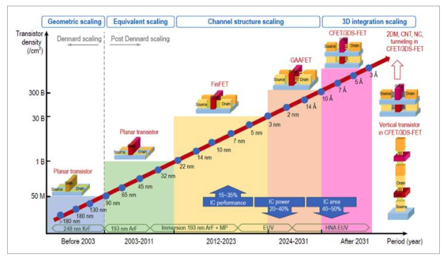
Doping in CMOS Scaling and Advanced Nodes
As ICs shrink below 10 nm, doping becomes unpredictable. This is not theory—it is physics fighting back.
Key challenges:
- Random Dopant Fluctuation (RDF) causes threshold variability
- Ultra-shallow junctions push process limits
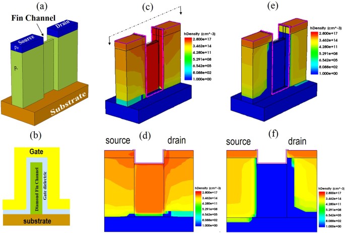
- 3D devices (FinFET, GAAFET) reduce reliance on heavy channel doping
Ironically, the future of scaling involves less doping in critical regions, replaced by geometry and electrostatics. But source/drain and well doping remain unforgiving.

Why Doping Knowledge Matters Across the IC Value Chain
Doping is not just an engineering topic. It is a strategic lever.
- Engineers need it for performance and reliability
- Executives need it to manage cost, yield, and risk
- Supply chain leaders need it to assess substitution, second sourcing, and long-term availability
A chip may look identical on paper. Same node. Same package. Same specs. But if doping control differs, behavior will diverge—sometimes catastrophically.
As an old manufacturing proverb warns: “The defect you don’t see is the one that fails in the field.”
Understanding doping helps prevent that failure.
Final Takeaway
Semiconductor doping is subtle. Silent. Ruthlessly important.
It shapes electrons. It defines transistors. It decides whether an IC succeeds—or quietly fails years later.
Those who understand doping control the outcome. Those who ignore it inherit the risk.
