


Leadframe vs Substrate Packaging: How to Choose the Right IC Package for Your Product
Integrated circuit (IC) packaging is not a back-end detail.
It is a strategic decision.
The right package can cut cost, boost reliability, and accelerate time-to-market.
The wrong one can quietly destroy margins, delay qualification, or break supply chains.
Among all options, leadframe packaging and substrate packaging remain the two dominant choices. They look similar from the outside. Inside, they are worlds apart.
This guide explains those differences—clearly, deeply, and practically—so you can choose with confidence.
1. Understanding IC Packaging and Why It Matters
IC packaging connects silicon to the real world. It protects the die, routes signals, removes heat, and allows automated assembly onto a PCB.
Packaging choices directly affect four business outcomes:
- Cost structure – material, assembly, yield, and test
- Performance – signal integrity, power delivery, frequency
- Reliability – thermal cycling, moisture resistance, field life
- Speed – design cycle, qualification, and ramp
As Intel’s Gordon Moore famously implied, “You can’t scale silicon without scaling everything around it.” Packaging is that “everything.”
In mature markets, packaging decisions often matter more than silicon features.
2. Historical Evolution and Industry Trends
Leadframe packaging came first. It powered decades of electronics growth—radios, TVs, PCs, and early mobile devices.
Substrate packaging emerged later, driven by:
- Smaller process nodes
- Rising I/O counts
- Higher data rates
- System-on-chip (SoC) complexity
Yet history matters. Leadframes never disappeared because economics still rule.
Today’s trend is polarized:
- High-volume, cost-sensitive products stay with leadframes
- High-performance computing (HPC), AI, networking, and automotive ADAS move to substrates
The market doesn’t choose one winner. It chooses fit.
3. What Is Leadframe Packaging?
Leadframe packaging uses a stamped or etched metal frame—usually copper alloy—to support the silicon die and form electrical leads.
Core Structure
- Copper leadframe
- Die attach (epoxy or solder)
- Wire bonds (gold, copper, or silver)
- Mold compound
Common Package Types
- DIP, SOP, SOIC
- QFP
- QFN / DFN
- SOT
Typical Applications
- Power management ICs
- Analog and mixed-signal devices
- MCUs for appliances and industrial control
- Automotive body and power electronics
Leadframes are simple, rugged, and proven.
4. Advantages and Limitations of Leadframe Packaging
Advantages
1. Cost efficiency
Leadframes are cheap to make and fast to assemble. Tooling is mature. Yield is high.
2. Thermal performance
Exposed-pad QFN packages offer excellent heat paths from die to PCB.
3. Supply chain stability
Thousands of OSATs support leadframes globally. Second sources are easy.
4. Mechanical robustness
They survive vibration, shock, and thermal cycling well—critical for automotive and industrial use.
Limitations
1. Limited I/O density
Wire bonding and lead pitch limit scalability.
2. Routing constraints
Signal paths are longer and less controlled.
3. High-frequency limits
Not ideal for GHz-class interfaces or dense power delivery networks.
In short: leadframes excel at value, not complexity.
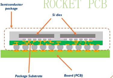
5. What Is Substrate Packaging?
Substrate packaging replaces the metal frame with a multilayer organic substrate, similar to a mini PCB.
Core Structure
- Build-up substrate (BT resin or Ajinomoto ABF)
- Redistribution layers (RDL)
- Flip-chip or wire-bond interconnect
- Solder balls or lands (BGA/LGA)
Common Package Types
- BGA
- LGA
- CSP
- Flip-Chip BGA
Typical Applications
- CPUs, GPUs, and AI accelerators
- Networking ASICs
- Mobile application processors
- High-end automotive SoCs
Substrates enable scale and speed.
6. Advantages and Limitations of Substrate Packaging
Advantages
1. High I/O density
Thousands of connections are possible.
2. Superior electrical performance
Shorter interconnects. Better impedance control. Lower parasitics.
3. Design flexibility
Supports advanced nodes, chiplets, and complex power delivery.
Limitations
1. Higher cost
Substrates, especially ABF, are expensive and capacity-constrained.
2. Manufacturing complexity
Flip-chip, underfill, and warpage control add risk.
3. Longer qualification cycles
More failure modes. More testing.
As the saying goes in semiconductor manufacturing:
“Every added layer is another place for something to go wrong.”
7. Thermal Performance and Reliability Comparison
Thermal behavior defines long-term reliability.
| Factor | Leadframe Packaging | Substrate Packaging |
|---|---|---|
| Heat path | Direct (die → leadframe → PCB) | Indirect (die → bumps → substrate → PCB) |
| Power density | Moderate | High |
| Junction temp control | Excellent for low–mid power | Better for very high power with heat spreaders |
| Automotive suitability | Excellent | Requires careful design |
For power ICs and harsh environments, leadframes often outperform expectations.
8. Volume Economics and Cost Breakdown
Cost is not just BOM. It is volume × yield × time.
| Cost Element | Leadframe | Substrate |
|---|---|---|
| Package material | Low | High |
| Assembly cost | Low | Medium–High |
| Yield risk | Low | Medium |
| Tooling NRE | Low | High |
| Best volume range | 1M–500M units | 10k–10M units |
Consumer electronics often tolerate substrate costs.
Industrial and automotive markets rarely do—unless performance demands it.
9. Leadframe vs Substrate: Side-by-Side Summary
| Dimension | Leadframe | Substrate |
|---|---|---|
| Cost | ★★★★★ | ★★☆☆☆ |
| I/O scalability | ★★☆☆☆ | ★★★★★ |
| Electrical performance | ★★☆☆☆ | ★★★★★ |
| Thermal efficiency | ★★★★☆ | ★★★☆☆ |
| Supply chain risk | Low | Medium–High |
| Time-to-market | Fast | Slower |
This table hides a truth: most products don’t need substrate performance.
10. How to Choose the Right IC Package for Your Product
The smartest teams ask the right questions first.
Choose Leadframe When:
- I/O count < 300
- Frequencies < 1 GHz
- Cost sensitivity is high
- Automotive or industrial qualification is required
- Long product lifecycle matters
Choose Substrate When:
- High-speed interfaces are mandatory
- I/O density drives system size
- Advanced nodes (<7 nm) are used
- Power integrity is critical
Strategic Advice
Do not overdesign packaging.
Performance unused is money wasted.
As Peter Drucker said:
“The best way to predict the future is to create it—but cheaply.”
Final Thoughts
Leadframe vs substrate is not a technology battle.
It is a business decision disguised as engineering.
Leadframes win on cost, reliability, and scale.
Substrates win on density, speed, and complexity.
The right choice aligns silicon capability, market needs, and supply chain reality.
Choose wisely. Your margins depend on it.
