

How to Use AD620: A Complete Practical Guide from Basics to Real-World Applications
The AD620 instrumentation amplifier has survived decades of technological change. Newer chips exist. Cheaper chips exist. Yet engineers still choose AD620. Why? Because it works. Quietly. Reliably. Precisely.
As Analog Devices famously emphasizes in its application notes: “Precision is not optional. It is designed.”
That philosophy is exactly what the AD620 delivers.
This guide is written for engineers, students, and serious makers who want real-world results—not theory alone. We focus on how to use AD620 correctly, avoid hidden traps, and design circuits that survive outside the lab.
What Is the AD620 Instrumentation Amplifier?
The AD620 is a low-noise, high-accuracy instrumentation amplifier designed to amplify tiny differential signals while rejecting noise and interference.
It is optimized for:
- Microvolt-to-millivolt signals
- Noisy environments
- Precision measurement systems
Unlike standard op-amps, the AD620 integrates laser-trimmed resistors, ensuring stable gain, excellent matching, and exceptional common-mode rejection.
Who should use it?
- Sensor interface designers
- Biomedical engineers
- Industrial measurement developers
- Data acquisition system builders
If your signal is small and your environment is noisy, AD620 is a strong choice.
Key Technical Features and Performance Advantages


The power of AD620 lies in contrast: extreme sensitivity with strong noise immunity.
Core Advantages
- Low input offset voltage: typically 50 µV
- Low noise: 9 nV/√Hz at 1 kHz
- High CMRR: up to 120 dB
- Gain range: 1 to 10,000 with one resistor
- Low power consumption
Why this matters
Noise hides truth. Offset distorts reality. AD620 minimizes both.
| Parameter | Typical Value | Why It Matters |
|---|---|---|
| Input Offset | 50 µV | Accurate DC measurement |
| CMRR | 120 dB | Rejects power-line noise |
| Gain Error | 0.15% | Predictable amplification |
| Supply Current | 1.3 mA | Battery-friendly designs |
Short sentence. Big impact.
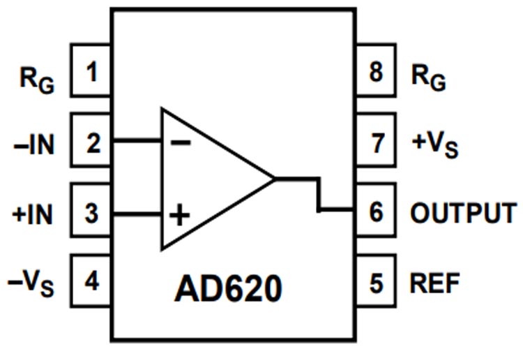
Understanding the AD620 Pinout and Internal Architecture

AD620 uses an 8-pin DIP or SOIC package, simple but powerful.
Key Pins Explained
- Pins 2 & 3 – Differential inputs
- Pin 6 – Output
- Pin 1 & 8 – Gain-setting resistor
- Pin 5 (REF) – Output reference level
- Pin 4 & 7 – Negative and positive supply
Internal Architecture (Simplified)
Inside, AD620 uses a three-op-amp topology:
- Two input buffers → high input impedance
- One differential amplifier → precision gain
Laser trimming ensures resistor matching that discrete designs cannot match.
Step-by-Step Guide: How to Use AD620 for the First Time


This is your “Hello World” moment.
1. Power It Correctly
- Dual supply: ±5 V to ±15 V (best performance)
- Single supply: +5 V or +3.3 V (requires biasing)
2. Set the Gain
One resistor. Two pins. That’s it.
[
\text{Gain} = 1 + \frac{49.4k\Omega}{R_G}
]
Example:
- RG = 499 Ω → Gain ≈ 100
3. Handle the REF Pin
- REF = 0 V → Output centered at ground (dual supply)
- REF = mid-supply → Required for single-supply operation
4. Verify Operation
- Use a multimeter for DC tests
- Use an oscilloscope for noise and bandwidth
If the output rails immediately, something is wrong. Stop and check.
Single-Supply vs Dual-Supply Operation
This is where many designs fail.
Single-Supply Operation (+5 V / +3.3 V)
Pros
- Simple power system
- Battery friendly
Cons
- Limited input common-mode range
- Output cannot swing to ground
Solution: Virtual ground (mid-supply bias).
Dual-Supply Operation (± Supplies)
Pros
- Full signal swing
- Easier design margins
- Better accuracy
Cons
- Extra power rail
Rule of thumb:
If accuracy matters, use dual supply.
How to Set Gain on the AD620 Correctly
Gain selection looks easy. It is. But mistakes are costly.
Practical Gain Examples
| Desired Gain | RG Value |
|---|---|
| 10 | 5.49 kΩ |
| 100 | 499 Ω |
| 1000 | 49.9 Ω |
Gain vs Bandwidth
Higher gain = lower bandwidth.
At Gain = 1 → ~120 kHz
At Gain = 1000 → ~1 kHz
Physics always collects its debt.
Common Mistakes
- Long wires to RG (adds noise)
- Cheap resistors (adds drift)
- Forgetting Kelvin connection
Typical AD620 Application Circuits


Sensor Interfaces
- Load cells
- Strain gauges
- Pressure sensors
Biomedical Signals
- ECG
- EMG
- EEG (with care)
Temperature Measurement
- Thermocouples
- RTDs
Data Acquisition
- Industrial DAQ front-ends
- Precision test equipment
The AD620 shines where signals whisper and noise screams.
Troubleshooting, Reliability, and Design Best Practices
Most AD620 failures are design errors, not chip failures.
Common Problems
- Output stuck at rail → common-mode violation
- Excessive noise → poor grounding
- Wrong gain → RG miscalculated
PCB Best Practices
- Symmetrical input routing
- Guard rings for high impedance
- Separate analog and digital grounds
- Place RG resistor close to pins
Reliability Notes
AD620 is mature, stable, and widely available. Its lifecycle is long. Its behavior is predictable. That matters in production.
As an old engineering proverb goes:
“The best amplifier is the one you don’t have to debug.”
Final Thoughts: When AD620 Is the Right Choice
The AD620 is not flashy. It is not new. It is not trendy.
It is trusted.
Choose AD620 when:
- Signal integrity matters
- Noise rejection is critical
- You want predictable, documented behavior
If you need rail-to-rail outputs, ultra-low power, or digital calibration, newer amplifiers may help. But when you need precision without surprises, AD620 still earns its place on the PCB.
Quiet. Accurate. Proven.
That is why engineers still use it.
