
How to Read Pinout Diagrams: A Practical Guide for Engineers & Decision-Makers
Pinout diagrams look simple. Boxes. Numbers. Labels.
Yet they quietly decide whether a product works flawlessly or fails catastrophically.
A single misread pin can burn silicon, delay launches, or force an expensive board re-spin. As the old engineering proverb goes: “Hardware is honest. It fails exactly where you misunderstood it.”
This guide strips away ambiguity. It shows engineers, technical managers, and sourcing leaders how to read pinout diagrams correctly, systematically, and safely—without guesswork.
What Is a Pinout Diagram and Why It Matters
A pinout diagram maps every physical pin on a component to its electrical function. It is the bridge between silicon intent and real-world wiring.
At its core, a pinout diagram shows:
- Physical pin numbers
- Orientation markers (Pin 1 reference)
- Electrical roles (power, ground, signal, control)
- Special conditions (NC, reserved, multiplexed)
Pinouts appear in datasheets, application notes, and vendor manuals. But they are not just for engineers.
They matter equally to procurement teams, quality managers, and decision-makers evaluating second sources or package changes.
“An error caught on paper costs pennies. An error caught on hardware costs millions.” — widely cited engineering management principle
Pinout literacy reduces risk across design, manufacturing, and supply chains.
Step 1: Identify the Correct Package Orientation
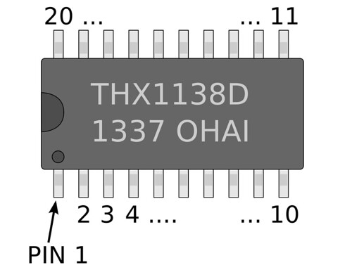
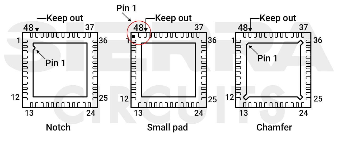
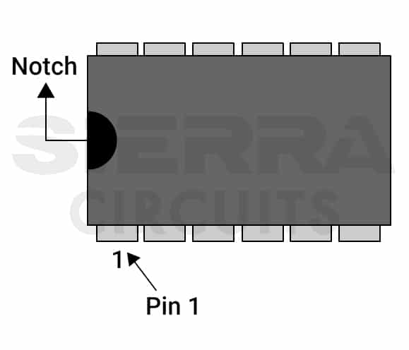
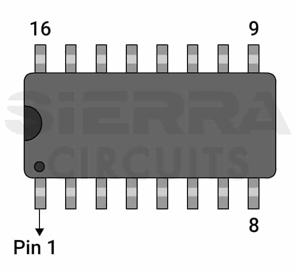
Orientation mistakes are the number one cause of catastrophic board failure.
Every pinout diagram assumes a specific viewing angle:
- Top view (most common)
- Bottom view (dangerous if overlooked)
Key Pin 1 Indicators
- Molded dot
- Laser-etched dot
- Notch or chamfer
- Missing ball or square pad (BGA/LGA)
Rotate the package incorrectly, and every signal shifts. Power lands on logic. Ground meets clock. Smoke follows.
Rule of thumb:
If orientation is unclear, stop. Cross-check photos, package drawings, and land patterns before routing.
Step 2: Understand Pin Numbering Conventions
Pin numbers follow logic—but not always intuition.
Most packages number pins counterclockwise, starting at Pin 1. But exceptions exist, especially in:
- BGA (row/column grids)
- LGA (matrix-based indexing)
- Custom power modules
| Package Type | Numbering Style | Common Risk |
|---|---|---|
| DIP / SOIC | Counterclockwise | Flipped footprint |
| QFN / QFP | Counterclockwise | Rotated land pattern |
| BGA | Grid-based (A1, B2…) | Axis inversion |
| LGA | Matrix + legend | Mirrored layout |
Pin numbering affects:
- Schematic symbols
- PCB footprints
- Pick-and-place data
- Automated inspection
A wrong assumption here multiplies downstream errors.
Step 3: Read and Interpret Pin Function Labels
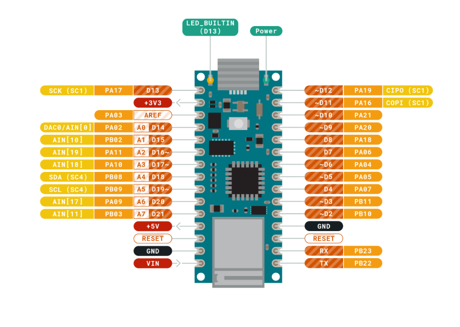
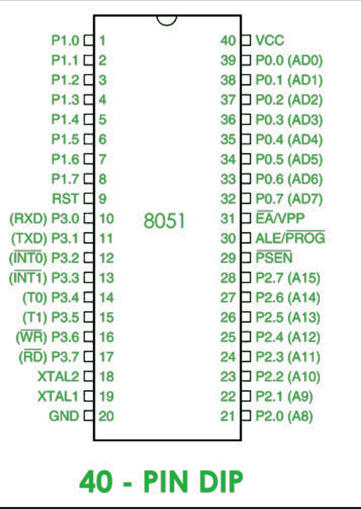
Not all pins are equal.
Core Categories
- Power pins: VCC, VDD, AVDD
- Ground pins: GND, AGND
- Signal pins: GPIO, data, address
- Control pins: EN, RESET, CLK
Identical pin counts do not imply compatibility. Two 64-pin ICs may share zero functional alignment.
Pin labels tell you:
- Electrical role
- Signal direction
- Domain membership (core vs I/O vs analog)
Always read pin names alongside electrical characteristics, not in isolation.
Step 4: Pin Multiplexing and Alternate Functions
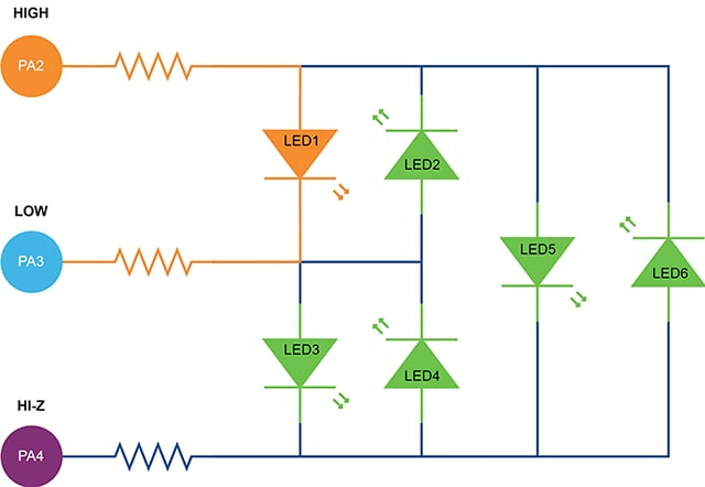


Modern ICs reuse pins aggressively.
One pin may act as:
- GPIO
- SPI clock
- UART TX
- Boot-mode selector
Why This Matters
- Default states at reset can conflict with hardware
- Software configuration may be required before safe operation
- External pull-ups or pull-downs may be mandatory
| Risk | Consequence |
|---|---|
| Ignoring default function | Boot failure |
| Overlapping peripherals | Signal contention |
| Missing pulls | Random behavior |
If a pin has alternate functions, assume danger until proven safe.
Step 5: Electrical Type, Direction, and Behavior
Understanding what a pin does is not enough. You must know how it behaves.
Common Electrical Types
- Input / Output / Bidirectional
- Push-pull
- Open-drain
- Analog-only
- Digital-only
Also consider behavior during:
- Reset
- Startup
- Sleep
- Fault conditions
Some outputs drive high at reset. Others float. Some pins source current; others only sink.
Design without this knowledge invites unpredictable failures.
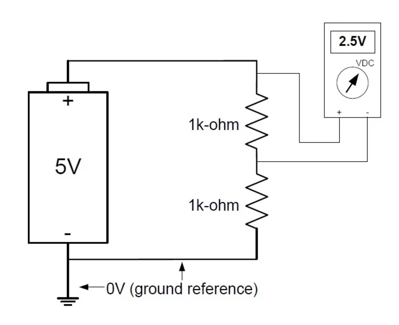
Step 6: Power Pins, Voltage Domains, and Sequencing
Power pins deserve obsessive attention.
Why so many VDD pins?
Because modern ICs isolate:
- Core logic
- I/O buffers
- Analog blocks
| Pin Type | Purpose |
|---|---|
| VDD / VCORE | Internal logic |
| VIO | Interface voltage |
| AVDD | Noise-sensitive analog |
| VBAT | Backup domain |
Pinouts often hint at power sequencing requirements. Clusters of pins. Separate grounds. Dedicated analog zones.
Miss the sequence, and the IC may degrade silently—or fail instantly.
Step 7: NC, Reserved, and Special-Handling Pins
NC does not always mean “ignore.”
Pin Types to Treat Carefully
- NC (No Connect): sometimes internally connected
- Reserved: future features or test hooks
- Strap pins: define modes at power-up
Floating pins are dangerous. Noise finds them. Logic misfires.
When unsure, follow the datasheet exactly. If it says “leave floating,” leave it floating. If it says “pull low,” pull low—always.
Step 8: Practical Review Checklists and Validation
The best engineers distrust assumptions.
Pinout Review Checklist
- Orientation verified against package drawing
- Pin numbers cross-checked with footprint
- Power and ground pins grouped logically
- Multiplexed pins reviewed with firmware team
- NC and reserved pins handled explicitly
Cross-reference:
- Pinout diagrams
- Pin tables
- Application schematics
- Reference designs
Use ECAD tools, but never rely on them blindly. Libraries fail too.
Why Pinout Knowledge Drives Smarter Decisions
Pinout mastery is not just technical hygiene. It is business leverage.
It enables:
- Faster second-source validation
- Safer package substitutions
- Lower re-spin risk
- Stronger supplier negotiations
Organizations that formalize pinout reviews ship faster and fail less.
Final Thoughts
Pinout diagrams are quiet documents. No drama. No flair.
Yet they sit at the fault line between success and failure.
Read them slowly. Question them deeply. Validate them relentlessly.
Because in hardware, what you misread today becomes what you debug tomorrow.
