
ESD Ratings for ICs and How to Test
Electrostatic discharge (ESD) is invisible. Silent. Fast.
Yet it is one of the most common root causes of integrated circuit (IC) failure—both in the lab and in the field.
As the proverb often attributed to Peter Drucker reminds us: “What gets measured gets managed.”
In ESD control, ratings and testing are how risk gets measured.
This guide explains what ESD ratings really mean, how IC ESD testing is performed, and why ratings alone are not enough. The goal is practical clarity—for engineers, quality teams, and buyers alike—at a readable, 7th-grade level.
What Is ESD and Why It Matters for IC Reliability
Electrostatic discharge is the sudden flow of electricity between two objects at different electrical potentials. A human walking across a floor can build thousands of volts. A machine arm can hold even more.
ICs, by contrast, are fragile.
Modern transistors use ultra-thin gate oxides and dense metal layers. These structures are measured in nanometers. ESD events are violent by comparison. A single discharge can punch through oxide, melt metal, or trigger latch-up.
The impact is not limited to engineering:
- Business: Scrap, rework, warranty returns
- Quality: Latent defects that escape testing
- Operations: Yield loss and line interruptions
- Procurement: Supplier risk and unclear specifications
In short: ESD failures are expensive, unpredictable, and often misdiagnosed.
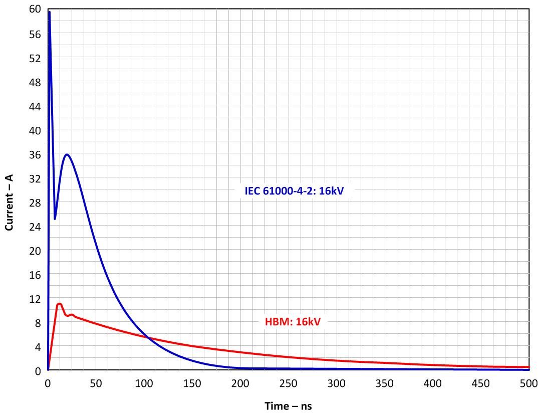
Common ESD Rating Models Used for Integrated Circuits
Three main models define how IC ESD robustness is measured. Each simulates a different real-world risk.
Human Body Model (HBM)
HBM simulates a charged person touching an IC pin. It uses a resistor and capacitor network to mimic human discharge.
- Typical ratings: 250 V to 4,000 V
- Historically dominant
- Still widely quoted in datasheets
HBM reflects handling during manual assembly or probing. It does not represent modern automated factories well.
Machine Model (MM)
MM simulates discharge from metallic equipment.
- Higher peak current than HBM
- Poor correlation to real events
- Largely deprecated
Most standards bodies no longer recommend MM because it overlaps with CDM and adds confusion.
Charged Device Model (CDM)
CDM represents a charged IC suddenly discharging to ground.
- Typical ratings: 125 V to 1,000 V
- Very fast rise times
- Extremely high peak currents
CDM is now the dominant risk for modern ICs—especially small packages and advanced nodes.
Typical ESD Rating Values and Industry Benchmarks
Not all ICs are created equal. ESD robustness varies by function, process node, and application.
Typical IC-Level ESD Ranges
| IC Type | Typical HBM | Typical CDM |
|---|---|---|
| MCU | 1–2 kV | 250–500 V |
| SoC / ASIC | 500–1,000 V | 125–250 V |
| Analog IC | 2–4 kV | 500–1,000 V |
| Power IC | 2–6 kV | 500–1,000 V |
Advanced nodes below 16 nm usually show lower CDM margins due to tighter geometries.
What Counts as Robust?
- Low: <500 V HBM or <125 V CDM
- Standard: 1 kV HBM, 250 V CDM
- Robust: ≥2 kV HBM, ≥500 V CDM
Industry Expectations
- Consumer: Cost-driven, moderate ESD
- Industrial: Higher margins, longer life
- Automotive: Strong ESD plus process control
How to Read and Interpret ESD Ratings on IC Datasheets
ESD ratings are often misunderstood—or misplaced.
They usually appear:
- In Absolute Maximum Ratings
- In Reliability or Handling sections
- Buried in footnotes
Key rules to remember:
- ESD ratings are not operating limits
- Passing a rating does not guarantee field immunity
- Pin combinations matter—but are rarely disclosed
Red flags include:
- “ESD compliant” with no numbers
- Missing CDM data
- Legacy MM ratings only
- Ratings tested on old packages
A wise saying from quality engineering applies here: “Absence of evidence is not evidence of absence.”
ESD Failure Mechanisms Inside Integrated Circuits
ESD damage is physical. It leaves scars.
Common Mechanisms
- Gate oxide breakdown: Permanent leakage or shorts
- Junction burnout: Localized heating destroys silicon
- Metal melt: Thin interconnects vaporize
- Snapback & latch-up: Triggered by fast ESD edges
Advanced nodes (FinFET, sub-10 nm) are more sensitive because:
- Oxides are thinner
- Margins are tighter
- Protection devices scale poorly
Some damage is catastrophic. Other damage is latent, waiting to fail months later.

Limitations of IC-Level ESD Ratings
A “2 kV HBM rated IC” can still fail in the field. This is not a paradox. It is physics.
Why?
- Lab tests are controlled and repeatable
- Real ESD events are chaotic
- System-level discharge paths are different
Another common confusion is ESD vs. EOS:
- ESD: Fast, high voltage, low energy
- EOS: Slower, high energy, often power-related
Mislabeling EOS as ESD leads to wrong fixes—and repeated failures.
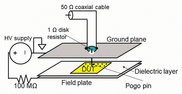
ESD Testing Standards and Compliance Requirements
ESD testing follows global standards to ensure consistency.
Key Organizations
- JEDEC – IC-level ESD standards
- IEC – System-level testing
Common Standards
| Level | Standard | Purpose |
|---|---|---|
| IC | JESD22-A114 | HBM |
| IC | JESD22-C101 | CDM |
| System | IEC 61000-4-2 | End-equipment ESD |
Pass/fail is based on no parametric shift and no functional loss after stress.
Modern standards emphasize CDM accuracy and lower voltage steps than legacy methods.
How ESD Testing for ICs Is Performed
ESD testing is systematic and unforgiving.
Typical Flow
- Control humidity and grounding
- Select worst-case pin combinations
- Apply positive and negative pulses
- Step voltage until failure or limit
- Re-test electrical parameters
Testing may occur:
- At wafer level (early screening)
- On packaged devices (qualification)
Latent damage often requires burn-in or extended testing to detect.

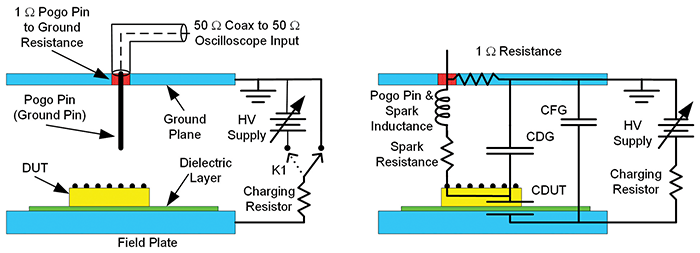

IC-Level vs. System-Level ESD Protection
This distinction is critical.
- IC ESD ratings protect the chip during handling
- System-level ESD protects the final product in use
IEC system tests involve:
- Contact discharge
- Air discharge
- Up to ±15 kV
Passing IC-level ESD does not ensure system compliance. External TVS diodes, layout control, and grounding are often required.
As reliability engineers say: “The system fails as a system—not as a component.”
Best Practices Summary
What Smart Teams Do
- Specify HBM and CDM clearly
- Focus on CDM risk for modern packages
- Audit handling and ESD control programs
- Combine IC ratings with system-level design
Key Takeaways
- ESD ratings measure survivability, not immunity
- CDM is the dominant modern threat
- Datasheets tell only part of the story
- Testing, handling, and system design must align
ESD is silent. But its message is loud:
Design for reality, not just for the rating.
