
Electrostatic Discharge (ESD) Protection Methods: A Practical Guide for Reliable Electronics
Electrostatic Discharge (ESD) is silent. Fast. Destructive.
It can strike without warning and leave no visible trace—yet the damage can be permanent.
As devices shrink and speeds increase, ESD tolerance drops. What worked ten years ago no longer works today. This guide cuts through theory and focuses on practical, system-level ESD protection that engineers can actually apply.
Short sentences. Clear logic. Real-world focus.


What Is Electrostatic Discharge (ESD) and Why It Matters
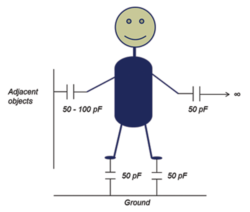
Electrostatic Discharge is the sudden transfer of electrical charge between objects at different potentials.
It happens in nanoseconds.
Voltages can exceed 15,000 V.
ESD is often confused with Electrical Overstress (EOS) or lightning surge. They are not the same.
Key Differences That Matter in Design
| Event Type | Duration | Energy | Typical Source | Common Damage |
|---|---|---|---|---|
| ESD | ns–µs | Low | Human, cable, connector | Gate oxide rupture |
| EOS | ms–s | High | Power fault, short | Melted metal |
| Surge | µs–ms | Very high | Lightning, grid | System failure |
Critical insight:
ESD protection alone does not protect against EOS.
Modern ICs have thinner oxides and tighter margins. One ESD hit can cause:
- Immediate failure
- Latent damage
- Parametric drift
As Benjamin Franklin warned centuries ago:
“An ounce of prevention is worth a pound of cure.”
In electronics, that ounce is ESD design.

Common ESD Damage Scenarios You Should Know
ESD damage is not always dramatic. That’s what makes it dangerous.
The Three Failure Modes
| Failure Type | When It Appears | Risk Level | Typical Symptom |
|---|---|---|---|
| Catastrophic | Immediate | Obvious | Device dead |
| Latent | Weeks or months | Severe | Random field failure |
| Parametric | Gradual | Hidden | Timing drift, leakage |
Latent failures are the most expensive.
They pass test.
They fail in the field.
That failure costs more than money. It costs trust.
On-Chip ESD Protection at the IC Level
Every IC has internal ESD protection.
But it is limited by design trade-offs.
Common On-Chip Protection Structures
- ESD diodes to VDD and GND
- Rail clamps triggered during fast transients
- SCR-based devices for high robustness
These structures must balance:
- Protection strength
- Leakage current
- Signal integrity
For high-speed interfaces, excessive capacitance is deadly.
For power pins, weak clamps invite EOS.
Golden rule:
Never rely on IC-level ESD protection alone.
It is your last line, not your first.

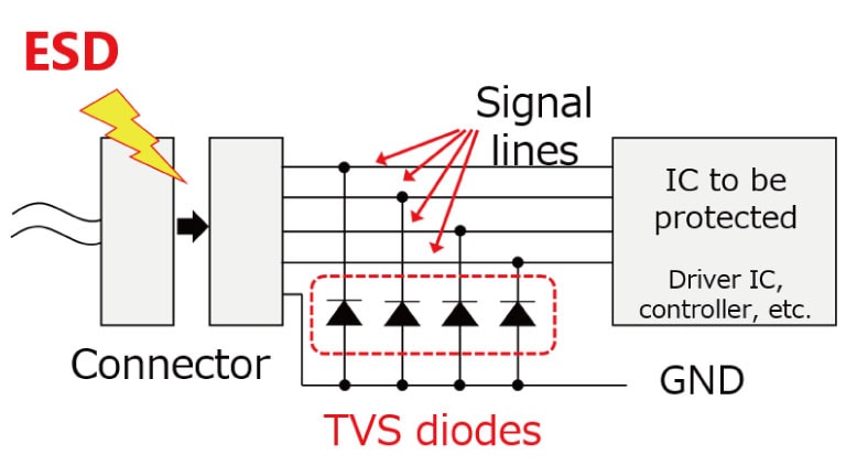
External ESD Protection Components for Interfaces
External protection absorbs energy before it reaches silicon.
Common Component Choices
| Component | Response Speed | Capacitance | Best Use |
|---|---|---|---|
| TVS diode | Very fast | Low–medium | USB, HDMI |
| Varistor | Moderate | High | Power lines |
| ESD array | Very fast | Ultra-low | High-speed data |
High-Speed Interface Protection
Interfaces like USB, HDMI, and Ethernet are exposed by design.
They act like antennas.
Place TVS diodes:
- As close to the connector as possible
- With the shortest ground return
- Before any routing splits
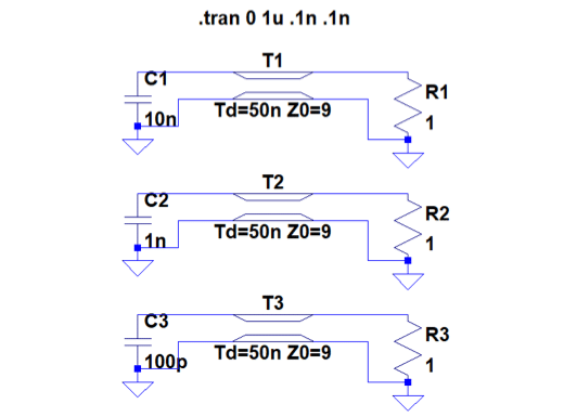
Cable Discharge Events (CDE)
Cables store charge.
When plugged in, they discharge violently.
CDE can exceed 30 A peak current.
Mitigation techniques:
- Series resistors
- Ferrite beads
- Dedicated CDE-rated TVS devices

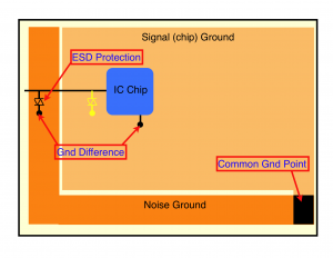
PCB Layout and System-Level ESD Design
ESD protection fails more often due to layout, not component choice.
Layout Rules That Actually Work
- Solid ground planes
- Short, wide return paths
- No stubs near connectors
- Controlled impedance for high-speed lines
Enclosure and Shielding Effects
| Enclosure Type | ESD Behavior | Risk Level |
|---|---|---|
| Plastic | Stores charge | High |
| Metal | Shunts charge | Lower |
| Coated plastic | Controlled | Medium |
Connector shields should:
- Bond to chassis ground
- Avoid sharing signal return paths
Most ESD failures happen at interfaces.
Design there first.
Software and Firmware-Level ESD Mitigation
Hardware reduces damage.
Software restores control.
Essential Firmware Strategies
- Watchdog timers
- Brown-out detection
- Automatic state recovery
After an ESD hit:
- Registers may corrupt
- I/O may latch
- State machines may stall
Logging ESD-related resets helps isolate root cause later.
Resilience is not optional.
It is part of reliability engineering.
ESD Protection in Key Applications
Different environments. Different risks.
Automotive Electronics
- ISO functional safety
- High transient exposure
- Long service life
Robust grounding and multi-stage protection are mandatory.
Industrial Systems
- Long cables
- High EMI
- Frequent human interaction
Isolation plus ESD protection is often required.
Consumer Electronics and IoT
- Cost pressure
- Thin enclosures
- High-volume production
Here, layout discipline matters more than expensive parts.
ESD Control in Manufacturing and Logistics
ESD does not start in the field.
It often starts in the factory.
Effective ESD Control Measures
- Grounded workstations
- Wrist straps and heel straps
- Conductive packaging
- Humidity control
A formal ESD program aligned with ANSI/ESD Association guidelines reduces yield loss and warranty returns.
Training matters.
Audits matter more.
ESD Testing, Standards, and Compliance
Testing validates design assumptions.
Key Test Models
| Model | Represents | Typical Use |
|---|---|---|
| HBM | Human touch | Component |
| CDM | Charged device | Component |
| IEC 61000-4-2 | Real system | End product |
System-level testing under IEC standards exposes weaknesses that lab simulations miss.
Test early.
Test often.
Cost vs. Protection Level Optimization
More protection is not always better.
Over-design:
- Adds capacitance
- Increases cost
- Hurts performance
Under-protection:
- Field failures
- Brand damage
- Recall risk
The goal is right-sized protection, based on:
- Use environment
- Interface exposure
- Failure cost
Wise engineers optimize risk—not fear it.
Emerging Trends and Future Challenges in ESD Protection
Advanced CMOS and FinFET technologies are less forgiving.
Voltages drop. Margins vanish.
Key trends:
- Ultra-low capacitance TVS
- Integrated ESD arrays
- Co-design of IC and system protection
ESD is no longer an afterthought.
It is a system architecture decision.
Conclusion: Designing a Holistic ESD Protection Strategy
ESD protection is not one component.
It is a discipline.
It spans:
- Silicon
- PCB
- Enclosure
- Firmware
- Manufacturing
When done right, it is invisible.
When done wrong, it is unforgettable.
Design for reality.
Design for reliability.
Design for the field—not the lab.
That is how robust electronics are built.
