CY7C1353G-133AXC Overview
The CY7C1353G-133AXC is a high-performance synchronous Static Random Access Memory (SRAM) designed for applications requiring fast access times and reliable data storage. Operating at a clock frequency of 133 MHz, this 32K x 8-bit memory device delivers efficient synchronous operation with a low power consumption profile. Its advanced architecture supports seamless integration into high-speed systems, providing deterministic timing for improved system performance. Ideal for industrial and embedded applications, the product ensures robust data handling and consistent operation across varying environments. For more detailed technical information and purchasing options, visit IC Manufacturer.
CY7C1353G-133AXC Technical Specifications
| Parameter | Specification |
|---|---|
| Memory Organization | 32K x 8 bits |
| Clock Frequency | 133 MHz |
| Access Time | 7.5 ns |
| Operating Voltage | 3.3 V ?? 0.3 V |
| Power Consumption (Active) | Max 180 mW |
| Interface Type | Synchronous SRAM |
| Package Type | 44-Pin TSOP II |
| Operating Temperature Range | -40??C to +85??C |
CY7C1353G-133AXC Key Features
- Synchronous Operation: Ensures precise timing control with external clock signals, enabling high-speed data transfer and system synchronization.
- High-Speed Access: 7.5 ns access time allows for rapid read/write cycles, improving overall system throughput in demanding applications.
- Low Voltage Operation: Operates at 3.3 V, reducing power consumption and supporting energy-efficient system designs.
- Compact 44-Pin TSOP II Package: Facilitates easy PCB layout and integration in space-constrained environments.
- Wide Temperature Range: Designed for industrial-grade applications with reliable operation from -40??C to +85??C.
- Robust Data Retention: Maintains data integrity with stable SRAM cells under varying electrical and thermal conditions.
CY7C1353G-133AXC Advantages vs Typical Alternatives
This memory device offers faster synchronous access compared to asynchronous SRAM alternatives, enabling higher system efficiency. Its low power consumption and industrial temperature tolerance make it a reliable choice for embedded systems and industrial controls. The compact TSOP II package simplifies board design, while the 3.3 V operation aligns with modern low-power system standards. Overall, it provides precise timing and robust performance where speed and reliability are critical.
🔥 Best-Selling Products
-
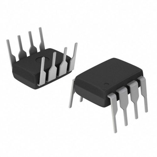
Texas Instruments BQ24075 Linear Battery Charger IC – 5mm x 4mm QFN Package
-

Texas Instruments INA219 Current Sensor Module – SOIC Package, Precision Monitoring
-

Texas Instruments LM4041 Precision Voltage Reference – SOT-23 Package
-

Texas Instruments OPA2134 Audio Op Amp – Dual, High-Performance, SOIC-8 Package
Typical Applications
- High-speed cache memory in networking and telecommunications equipment, where synchronous data access and fast read/write cycles improve throughput and latency.
- Embedded systems requiring reliable, low-power SRAM for buffering and temporary data storage in industrial automation.
- Data storage in digital signal processing (DSP) systems that demand deterministic timing and rapid data retrieval.
- Consumer electronics and computing devices utilizing synchronous SRAM for system memory expansion and performance enhancement.
CY7C1353G-133AXC Brand Info
This device is part of the CY7C1353G series, well-regarded for its synchronous SRAM technology. Manufactured to meet stringent quality and reliability standards, the product aligns with industry demands for fast, low-power, and durable memory solutions. The series supports diverse industrial and embedded applications, ensuring compatibility and performance consistency. The CY7C1353G-133AXC reflects a commitment to advanced semiconductor design and manufacturing excellence.
FAQ
What is the significance of the 133 MHz clock frequency in this SRAM?
The 133 MHz clock frequency defines the maximum synchronous operating speed of the device, allowing it to perform read and write operations aligned with an external clock signal. This enables higher data throughput and precise timing control, which are critical for high-speed applications.
🌟 Featured Products
-

“Buy MAX9312ECJ+ Precision Voltage Comparator in DIP Package for Reliable Performance”
-

QCC-711-1-MQFN48C-TR-03-1 Bluetooth Audio SoC with MQFN48C Package
-

0339-671-TLM-E Model – High-Performance TLM-E Package for Enhanced Functionality
-
1-1415898-4 Connector Housing, Electrical Wire-to-Board, Receptacle, Packaged
How does the synchronous interface improve system performance?
A synchronous interface ensures that all memory operations are synchronized with an external clock. This coordination reduces wait states and timing uncertainty, resulting in faster and more predictable data access compared to asynchronous SRAM devices.
What are the power consumption characteristics of this memory component?
The device operates at 3.3 V with

