CY74FCT2541TQC Overview
The CY74FCT2541TQC is a high-performance, 10-bit registered transceiver designed for advanced data bus applications. Featuring dual 5-bit buses and registered outputs, this device combines fast propagation delays with low power consumption, making it ideal for synchronous systems requiring reliable data storage and transfer. Its robust architecture supports bus-oriented systems with precise timing control, enhancing signal integrity and system stability. The device is manufactured with advanced CMOS technology, ensuring compatibility with a wide range of voltage levels and operating conditions. For detailed technical insights and sourcing information, visit IC Manufacturer.
CY74FCT2541TQC Technical Specifications
| Parameter | Specification |
|---|---|
| Logic Function | 10-bit Registered Transceiver (Dual 5-bit buses) |
| Operating Voltage (Vcc) | 4.5 V to 5.5 V |
| Propagation Delay (tpd) | Typically 3.5 ns |
| Output Enable (OE) | Active Low Control Inputs |
| Data Inputs | Registered on Clock (CLK) Signal |
| Package Type | 44-Lead Thin Quad Flat Package (TQFP) |
| Input Clamp Diode Current | ??20 mA Maximum |
| Operating Temperature Range | -40??C to +85??C |
| Power Dissipation | Maximum 1.0 W |
CY74FCT2541TQC Key Features
- Registered 10-bit transceiver architecture: Enables simultaneous 5-bit data transfers in both directions with output data registered on the rising edge of the clock, providing improved data timing and system synchronization.
- Low propagation delay: Fast switching speeds (typically 3.5 ns) ensure minimal latency, critical for high-speed bus interfacing and timing-sensitive applications.
- Advanced CMOS technology: Offers low power consumption and enhanced noise immunity, contributing to overall system reliability and reduced heat generation.
- Output enable control: Active low OE inputs provide flexible bus control, allowing easy integration into multiplexed or shared bus systems.
CY74FCT2541TQC Advantages vs Typical Alternatives
This device excels over typical alternatives by combining registered outputs with dual 5-bit transceiver functionality, delivering superior timing control and data integrity. Its low propagation delay and low power CMOS design enhance performance and energy efficiency. The integrated output enable controls further simplify system design, making it a reliable choice for synchronous bus interfacing in demanding industrial or communication environments.
🔥 Best-Selling Products
-
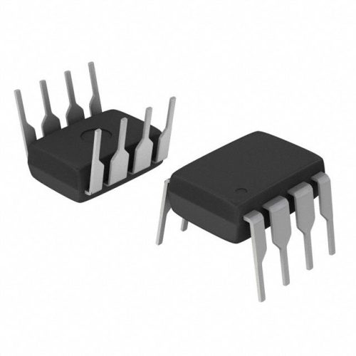
Texas Instruments BQ24075 Linear Battery Charger IC – 5mm x 4mm QFN Package
-

Texas Instruments INA219 Current Sensor Module – SOIC Package, Precision Monitoring
-

Texas Instruments LM4041 Precision Voltage Reference – SOT-23 Package
-

Texas Instruments OPA2134 Audio Op Amp – Dual, High-Performance, SOIC-8 Package
Typical Applications
- Data bus interfacing in synchronous digital systems where fast, reliable 10-bit data transfer with registered control is essential for maintaining signal integrity and timing accuracy.
- High-speed memory address and data buffering to improve system throughput and reduce timing skew in complex microprocessor environments.
- Peripheral device interface circuits requiring bidirectional data flow with controlled output enabling for safe bus sharing.
- Industrial control systems that demand robust, low-power registered transceivers for reliable communication between modules operating in noisy environments.
CY74FCT2541TQC Brand Info
The CY74FCT2541TQC is part of a family of high-performance logic devices from a leading semiconductor manufacturer known for delivering reliable, industry-standard components. Designed with precision and stringent quality controls, this registered transceiver supports modern digital architectures with consistent performance. The brand??s reputation for innovation in CMOS technology ensures the device meets the rigorous demands of industrial and communication applications, backed by extensive documentation and global support channels.
FAQ
What is the primary function of the CY74FCT2541TQC?
This device functions as a 10-bit registered transceiver with dual 5-bit buses, enabling bidirectional data transfer with output data registered on the clock signal. It is designed to synchronize data flow and improve timing control in bus-oriented digital systems.
🌟 Featured Products
-

“Buy MAX9312ECJ+ Precision Voltage Comparator in DIP Package for Reliable Performance”
-
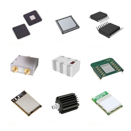
QCC-711-1-MQFN48C-TR-03-1 Bluetooth Audio SoC with MQFN48C Package
-

0339-671-TLM-E Model – High-Performance TLM-E Package for Enhanced Functionality
-
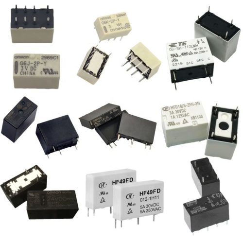
1-1415898-4 Connector Housing, Electrical Wire-to-Board, Receptacle, Packaged
What are the voltage and temperature operating ranges for reliable use?
The device operates reliably

