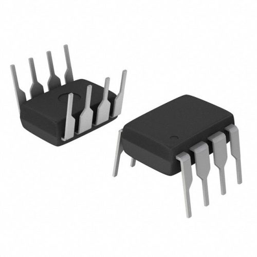
CY74FCT16244ATPAC Overview
The CY74FCT16244ATPAC is a high-performance 16-bit transceiver designed for asynchronous two-way communication between data buses. Featuring a 3-state output capability and operating at 3.3 V, this device supports bidirectional data flow with separate output-enable controls, making it ideal for bus-oriented applications requiring efficient data management. The device incorporates advanced Fast CMOS Technology (FCT) to deliver low propagation delay and reduced power consumption. Reliable and versatile, it integrates seamlessly into complex digital systems, ensuring robust data transfer and system integrity. For detailed technical insights and sourcing, refer to IC Manufacturer.
CY74FCT16244ATPAC Technical Specifications
| Parameter | Specification |
|---|---|
| Logic Function | 16-bit bus transceiver with 3-state outputs |
| Operating Voltage (Vcc) | 3.3 V ?? 0.3 V |
| Propagation Delay (tPD) | 5.5 ns (typical) |
| Maximum Clock Frequency | Up to 125 MHz (device speed compatible) |
| Output Drive | ??24 mA at 3.3 V |
| Input Voltage High (VIH) | 2.0 V (minimum) |
| Input Voltage Low (VIL) | 0.8 V (maximum) |
| Package Type | 44-pin Thin Quad Flat Package (TQFP) |
| Operating Temperature Range | -40??C to +85??C |
CY74FCT16244ATPAC Key Features
- 16-bit bidirectional data bus transceiver: Enables efficient two-way communication between buses, simplifying data routing in complex systems.
- Separate output-enable controls: Allows independent control of data flow direction, improving system flexibility and preventing bus contention.
- Fast CMOS Technology (FCT): Ensures low propagation delay (~5.5 ns), enhancing overall system speed and timing accuracy.
- High output drive capability: Supports ??24 mA output current, suitable for driving large bus loads without external buffering.
- 3.3 V low-voltage operation: Reduces power consumption while maintaining compatibility with modern low-voltage digital logic levels.
- 3-state outputs: Provides high-impedance state for bus sharing and system isolation during inactive periods.
- Wide operating temperature range: Reliable performance from -40??C to +85??C for industrial and commercial applications.
CY74FCT16244ATPAC Advantages vs Typical Alternatives
This transceiver stands out from typical alternatives due to its low-voltage 3.3 V operation combined with high output drive and fast switching speeds. The separate output-enable controls provide precise bus management, reducing risk of contention and improving signal integrity. Its robust FCT architecture delivers higher speed performance and lower power dissipation compared to older TTL or standard CMOS devices, making it a reliable choice for high-density, speed-sensitive industrial and embedded applications.
🔥 Best-Selling Products
-

Texas Instruments BQ24075 Linear Battery Charger IC – 5mm x 4mm QFN Package
-

Texas Instruments INA219 Current Sensor Module – SOIC Package, Precision Monitoring
-

Texas Instruments LM4041 Precision Voltage Reference – SOT-23 Package
-

Texas Instruments OPA2134 Audio Op Amp – Dual, High-Performance, SOIC-8 Package
Typical Applications
- Data bus interfacing in high-speed digital systems, enabling controlled bidirectional data transfer across multiple subsystems.
- Memory address and data bus buffering where isolation and timing control are critical.
- Microprocessor and microcontroller peripheral communication requiring 16-bit wide data paths.
- Industrial automation equipment and control systems demanding reliable, low-power bus transceivers.
CY74FCT16244ATPAC Brand Info
The CY74FCT16244ATPAC is part of an established product line offering high-speed Fast CMOS (FCT) logic solutions widely used in industrial and commercial digital systems. Known for combining low power consumption with advanced bus interfacing capabilities, this device meets stringent requirements for timing precision and signal integrity. Its robust design and package options cater to engineers seeking optimal performance in 3.3 V bus transceiver applications across various sectors, from embedded systems to complex automation platforms.

