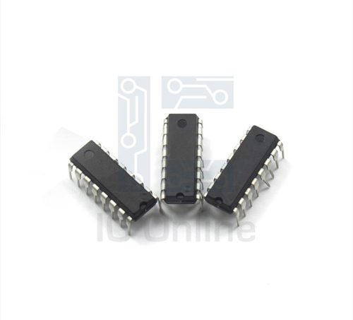
DDTC124TCA-7-F Overview
The DDTC124TCA-7-F is a high-performance dual NPN transistor designed for efficient switching and amplification in industrial and consumer electronics. Featuring matched transistor pairs with complementary electrical characteristics, it simplifies circuit design and enhances signal integrity. This device offers robust gain bandwidth and low noise, making it ideal for analog signal processing and driver applications. Packaged in a compact SOT-363 form factor, it supports high-density PCB layouts while maintaining reliable thermal performance. Available from IC Manufacturer, the DDTC124TCA-7-F delivers consistent quality for demanding electronic designs requiring precision and durability.
DDTC124TCA-7-F Technical Specifications
| Parameter | Value |
|---|---|
| Transistor Type | Dual NPN |
| Package | SOT-363 (SC-70-6) |
| Collector-Emitter Voltage (VCEO) | 30 V |
| Collector Current (IC) | 100 mA (continuous) |
| Current Gain (hFE) | 100 to 300 (typical) |
| Transition Frequency (fT) | 150 MHz (typical) |
| Power Dissipation (PD) | 300 mW |
| Operating Temperature Range | -55??C to +150??C |
| Input Capacitance (Cies) | 4 pF (typical) |
| Pin Configuration | Emitter, Base, Collector per transistor |
DDTC124TCA-7-F Key Features
- Dual matched NPN transistors: Ensures consistent gain and switching speeds, simplifying differential amplifier and switching circuit designs.
- High transition frequency (150 MHz): Supports high-speed switching and low distortion in analog signal processing, critical for RF and communication circuits.
- Compact SOT-363 package: Enables space-saving PCB layouts without compromising thermal performance, ideal for densely populated industrial boards.
- Wide operating temperature range: Suitable for harsh environmental conditions, enhancing reliability in automotive and industrial applications.
- Low input capacitance: Minimizes signal loss and switching delay, improving overall circuit efficiency and response time.
DDTC124TCA-7-F Advantages vs Typical Alternatives
This transistor pair stands out with its balanced electrical characteristics and high-frequency performance, offering greater precision than discrete transistor solutions. Its matched pair configuration reduces design complexity and improves signal symmetry. The low power dissipation and compact SOT-363 package provide advantages in energy efficiency and PCB space utilization, outperforming many conventional dual transistors in industrial and communication applications.
🔥 Best-Selling Products
-
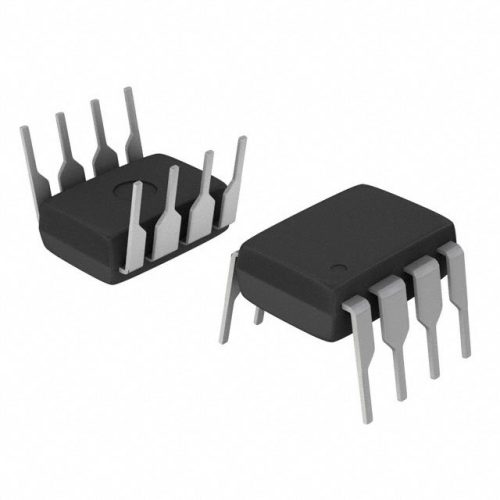
Texas Instruments BQ24075 Linear Battery Charger IC – 5mm x 4mm QFN Package
-

Texas Instruments INA219 Current Sensor Module – SOIC Package, Precision Monitoring
-

Texas Instruments LM4041 Precision Voltage Reference – SOT-23 Package
-

Texas Instruments OPA2134 Audio Op Amp – Dual, High-Performance, SOIC-8 Package
Typical Applications
- Differential amplifier stages in analog signal processing, where matched transistor pairs ensure accurate gain and low distortion for precise measurements.
- High-speed switching circuits in telecommunications equipment, leveraging the device??s high transition frequency for efficient data transmission.
- Driver stages for LEDs and small motors, benefiting from low power dissipation and compact packaging to optimize board layout.
- General-purpose amplification in consumer electronics, providing reliable performance across a broad temperature range for diverse operating conditions.
DDTC124TCA-7-F Brand Info
The DDTC124TCA-7-F is a product of a reputable semiconductor manufacturer known for quality discrete components and integrated circuits tailored for industrial and consumer markets. This transistor pair embodies the brand??s commitment to delivering reliable, high-performance components designed for demanding applications. Its consistent manufacturing standards and thorough quality control ensure long-term stability and compatibility with a wide array of electronic systems, reflecting the brand??s expertise in transistor technology.
FAQ
What is the primary function of this dual transistor package?
The dual transistor package integrates two NPN transistors matched for gain and frequency characteristics. This configuration simplifies circuit design in differential amplifiers, switching, and driver stages by providing balanced and consistent transistor pairs within a compact footprint.
🌟 Featured Products
-

“Buy MAX9312ECJ+ Precision Voltage Comparator in DIP Package for Reliable Performance”
-
QCC-711-1-MQFN48C-TR-03-1 Bluetooth Audio SoC with MQFN48C Package
-

0339-671-TLM-E Model – High-Performance TLM-E Package for Enhanced Functionality
-
1-1415898-4 Connector Housing, Electrical Wire-to-Board, Receptacle, Packaged
What are the voltage and current limits for safe operation?
The maximum collector-emitter voltage is 30 volts, and the continuous collector current rating is 100 milliamps per transistor. Operating within these limits ensures the device maintains optimal performance and longevity without risk of damage.

