SY89537LMY Overview
The SY89537LMY is a high-performance, low-jitter clock and data recovery device designed to enhance data integrity in high-speed communication systems. With its advanced features, it provides reliable synchronization for various applications, ensuring optimal performance and minimal signal degradation. This device caters to the demands of modern electronic designs, making it a preferred choice for engineers seeking robust solutions in data transmission. For further details, visit IC Manufacturer.
SY89537LMY Key Features
- Low jitter performance ensures high signal quality, reducing errors in data transmission.
- Integrated clock recovery supports a wide range of frequencies, providing flexibility in application design.
- High sensitivity enhances performance in noisy environments, making it ideal for critical communication systems.
- Compact design allows for easy integration into space-constrained applications, improving overall system efficiency.
SY89537LMY Technical Specifications
| Parameter | Value |
|---|---|
| Supply Voltage | 3.3V |
| Operating Temperature Range | -40??C to +85??C |
| Jitter Performance | Sub 1ps RMS |
| Input Frequency Range | 1MHz to 1.5GHz |
| Output Frequency Range | Up to 1.5GHz |
| Data Rate | Up to 3.125 Gbps |
| Package Type | QFN |
| Pin Count | 32 |
SY89537LMY Advantages vs Typical Alternatives
This device stands out against typical alternatives due to its superior low jitter characteristics and high sensitivity. These features ensure enhanced data integrity and reliability in high-speed applications, making it suitable for a variety of demanding environments.
🔥 Best-Selling Products
-
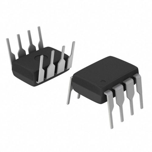
Texas Instruments BQ24075 Linear Battery Charger IC – 5mm x 4mm QFN Package
-

Texas Instruments INA219 Current Sensor Module – SOIC Package, Precision Monitoring
-

Texas Instruments LM4041 Precision Voltage Reference – SOT-23 Package
-

Texas Instruments OPA2134 Audio Op Amp – Dual, High-Performance, SOIC-8 Package
Typical Applications
- High-speed communication systems benefit from its clock recovery capabilities, ensuring accurate data transmission over long distances.
- Networking equipment utilizes this device for reliable signal processing, improving overall network performance.
- Data centers rely on its low jitter performance to maintain data integrity in critical applications.
- Broadcast systems employ this device to ensure synchronization in video and audio signal transmission.
SY89537LMY Brand Info
The SY89537LMY is manufactured by a reputable company known for its commitment to high-quality semiconductor solutions. The brand emphasizes innovation and reliability in its product line, catering to the evolving needs of the electronics industry. This device exemplifies the brand’s dedication to delivering advanced technology for high-performance applications.
FAQ
What is the primary use of the SY89537LMY?
The SY89537LMY is primarily used in high-speed communication systems where precise clock recovery and minimal jitter are essential for maintaining data integrity and performance in signal transmission.
🌟 Featured Products
-

“Buy MAX9312ECJ+ Precision Voltage Comparator in DIP Package for Reliable Performance”
-
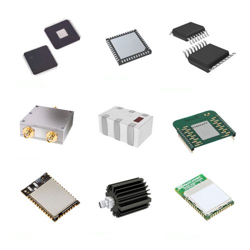
QCC-711-1-MQFN48C-TR-03-1 Bluetooth Audio SoC with MQFN48C Package
-

0339-671-TLM-E Model – High-Performance TLM-E Package for Enhanced Functionality
-
1-1415898-4 Connector Housing, Electrical Wire-to-Board, Receptacle, Packaged
Can the SY89537LMY operate in extreme temperatures?
Yes, this device is designed to operate effectively in a wide temperature range of -40??C to +85??C, making it suitable for various industrial and outdoor applications.
What types of applications can benefit from the SY89537LMY?
Applications such as networking equipment, data centers, and broadcast systems can significantly benefit from the performance enhancements provided by this high-speed clock and data recovery device.
📩 Contact Us
How does the SY89537LMY ensure low jitter performance?
The SY89537LMY utilizes advanced design techniques and technology to achieve sub 1ps RMS jitter performance, which is crucial for maintaining signal quality in high-speed data communications.
What package type does the SY89537LMY come in?
This device is offered in a compact QFN package, which facilitates easy integration into various electronic designs while saving valuable board space.

