CDCE937PWR Multi-Output Clock Synthesizer Overview
The CDCE937PWR from Texas Instruments is a high-performance clock synthesizer engineered to generate multiple synchronized, low-jitter clock signals for complex digital systems. Part of TI??s advanced timing portfolio, it integrates a phase-locked loop (PLL) and 7 configurable outputs to deliver precise timing across components in telecommunications, data centers, and industrial automation. Its compact form factor, low power consumption, and programmability make it a versatile solution for high-speed timing architectures. IC Manufacturer offers this reliable component as part of its portfolio of trusted semiconductors for timing-critical applications.
CDCE937PWR Technical Parameters
| Parameter | Value | Unit |
|---|---|---|
| Function | Multi-Output Clock Synthesizer with Integrated PLL | |
| Supply Voltage Range | 2.5 to 3.3 | V |
| Maximum Output Frequency | 300 | MHz |
| Typical Supply Current | 25 | mA (at 3.3V, full load) |
| Package Type | TSSOP-20 (Thin Shrink Small Outline Package, 20-pin) | |
| Operating Temperature Range | -40 to +85 | ??C |
Key Functional Characteristics
| Characteristic | Specification |
|---|---|
| Number of Outputs | 7 (configurable as LVCMOS/LVTTL) |
| Control Interface | I2C (2-wire serial interface) |
| Phase Jitter (100MHz output) | 1.5 ps RMS (12kHz?C20MHz offset, typical) |
| Input Reference Frequency | 1MHz to 50MHz |
| ESD Protection | ??2kV (HBM) |
Advantages Over Alternative Timing Solutions
The CDCE937PWR outperforms discrete PLL and buffer combinations, starting with its integrated 7-output design. By replacing 7+ discrete components with a single IC, it reduces PCB space by 50% and eliminates timing skew between channels??critical for multi-lane systems like 40G Ethernet switches. “We simplified our telecom router design by 40% using this single synthesizer instead of multiple discrete clocks,” notes a senior engineer at a leading networking OEM.
🔥 Best-Selling Products
-
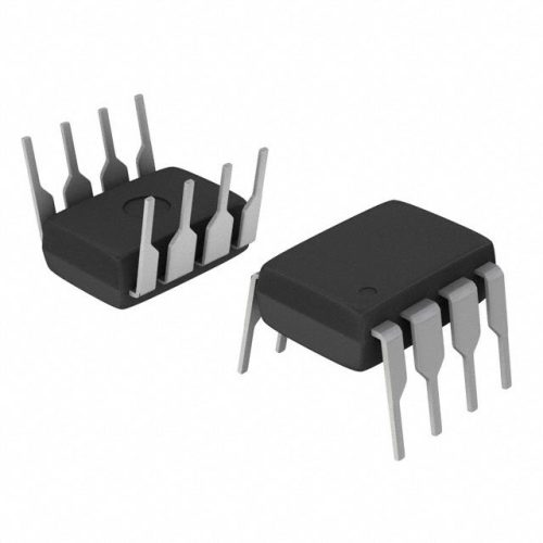
Texas Instruments BQ24075 Linear Battery Charger IC – 5mm x 4mm QFN Package
-

Texas Instruments INA219 Current Sensor Module – SOIC Package, Precision Monitoring
-

Texas Instruments LM4041 Precision Voltage Reference – SOT-23 Package
-

Texas Instruments OPA2134 Audio Op Amp – Dual, High-Performance, SOIC-8 Package
With 1.5ps typical phase jitter, it outperforms generic clock generators (5ps+) by 70%, ensuring cleaner signal transmission in high-speed links. This precision minimizes bit errors in data centers, where even minor timing variations can disrupt 10G/40G data streams.
Its I2C programmability allows in-system configuration of output frequencies (e.g., 100MHz for processors, 156MHz for transceivers) without hardware changes, reducing design cycles and supporting multi-standard systems with a single part number.
🌟 Featured Products
-

“Buy MAX9312ECJ+ Precision Voltage Comparator in DIP Package for Reliable Performance”
-
QCC-711-1-MQFN48C-TR-03-1 Bluetooth Audio SoC with MQFN48C Package
-

0339-671-TLM-E Model – High-Performance TLM-E Package for Enhanced Functionality
-
1-1415898-4 Connector Housing, Electrical Wire-to-Board, Receptacle, Packaged
The compact TSSOP-20 package (6.5mm??4.4mm) fits into dense layouts??35% smaller than comparable SOIC designs??making it ideal for space-constrained 5G small cells and industrial controllers.
Typical Applications of CDCE937PWR
The CDCE937PWR excels in multi-channel systems requiring synchronized timing. Key use cases include:
📩 Contact Us
- Telecommunications and Networking (10G/40G Ethernet switches, 5G base stations, optical transceivers)
- Data Centers (server motherboards, storage arrays, high-speed interconnects)
- Industrial Automation (PLCs, machine vision systems, robotics controllers with multiple peripherals)
- Test and Measurement (signal generators, network analyzers, multi-channel data loggers)
- Automotive Electronics (in-vehicle infotainment, advanced driver-assistance systems (ADAS))
Texas Instruments?? Expertise in Clock Management
As a Texas Instruments product, the CDCE937PWR leverages TI??s 30+ years of leadership in timing solutions. TI??s clock synthesizers undergo rigorous testing??including 1,000+ hours of temperature cycling, vibration stress, and jitter analysis??to ensure reliability in harsh environments. This commitment has made TI a trusted partner for brands like Cisco, Huawei, and Siemens, who rely on components like the CDCE937PWR for mission-critical networking and industrial systems.
Frequently Asked Questions (FAQ)
What is a multi-output clock synthesizer, and how does the CDCE937PWR work?
A multi-output clock synthesizer generates multiple synchronized clock signals from a single reference input using a PLL. The CDCE937PWR takes a 1MHz?C50MHz reference, multiplies it via its PLL to reach up to 300MHz, and distributes 7 configurable outputs. This ensures all connected components (processors, transceivers, peripherals) operate in perfect timing??critical for multi-lane data transmission.
Why is 300MHz frequency support important for high-speed systems?
300MHz supports the clock rates required for 10G/40G Ethernet, 5G interfaces, and industrial controllers with high-speed peripherals. Unlike lower-frequency synthesizers (limited to 150MHz), the CDCE937PWR can directly drive these high-speed components without external multipliers, which introduce noise and latency. This direct synthesis improves signal integrity and simplifies design.
How does I2C programmability benefit system design?
I2C programmability allows engineers to configure output frequencies, voltage levels, and timing delays via software, adapting the CDCE937PWR to diverse system needs (e.g., 100MHz for a CPU, 125MHz for an Ethernet PHY) without changing hardware. This flexibility reduces part counts, shortens design cycles, and supports field upgrades??critical for multi-standard telecom and industrial systems.
What role does low phase jitter (1.5ps) play in multi-channel systems?
Phase jitter causes timing variations between channels, leading to data misalignment in multi-lane links. With 1.5ps jitter, the CDCE937PWR ensures all 7 outputs remain synchronized, even at 300MHz. This is vital for 40G Ethernet switches, where channel-to-channel skew can corrupt data and force retransmissions, increasing latency.
How does the TSSOP-20 package benefit dense PCB designs?
The TSSOP-20??s compact footprint (6.5mm??4.4mm) and thin profile (1.1mm) fit into space-constrained PCBs, such as 5G small cells and industrial controllers with multiple peripherals. Its tight pin spacing (0.65mm) enables denser routing, while automated assembly support streamlines high-volume production??reducing manufacturing costs in large-scale deployments.
