Overview: TPS53432 High-Efficiency Synchronous Buck Converter
The TPS53432 from Texas Instruments is a synchronous step-down converter that simplifies power supply design for mid-range current applications. Featuring integrated MOSFETs, compact packaging, and support for wide input voltage ranges, it offers exceptional power efficiency in compact electronic systems.
Targeting embedded, networking, and telecommunications systems, the converter delivers a steady output of up to 6A while maintaining high efficiency (>90%). Its thermal and voltage protections add robustness to designs requiring stability and compactness.
🔥 Best-Selling Products
-
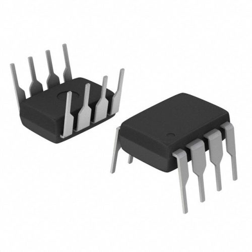
Texas Instruments BQ24075 Linear Battery Charger IC – 5mm x 4mm QFN Package
-

Texas Instruments INA219 Current Sensor Module – SOIC Package, Precision Monitoring
-

Texas Instruments LM4041 Precision Voltage Reference – SOT-23 Package
-

Texas Instruments OPA2134 Audio Op Amp – Dual, High-Performance, SOIC-8 Package
Key Electrical Specifications
| Parameter | Specification |
|---|---|
| Input Voltage Range | 4.5V ?C 18V |
| Output Current | Up to 6A |
| Switching Frequency | 200kHz ?C 1MHz (adjustable) |
| Efficiency | >90% |
| Package Type | QFN-20 |
| Protection | OCP, OTP, UVLO |
Why Choose TPS53432 Over Traditional Power Regulators?
Conventional switching regulators often require external components, which add to layout complexity and cost. The TPS53432 integrates high- and low-side FETs and control circuitry within a compact QFN-20 package. This not only saves space but also increases reliability and reduces EMI. Thanks to its adjustable frequency and comprehensive protection features, this IC offers better control and resilience compared to discrete solutions. Available from IC Manufacturer, it represents a reliable choice for engineers seeking proven performance.
Extended Technical Table
| Feature | Details |
|---|---|
| Control Topology | Voltage-Mode Control |
| Output Voltage Range | 0.6V to 5.5V |
| Output Type | Adjustable |
| Operating Temp Range | -40??C to 85??C |
| Synchronous FETs | Integrated |
| External Clock Sync | Yes |
Typical Application Areas
- Telecom base stations
- Data center boards for servers and storage
- FPGA and ASIC core supply in embedded systems
Frequently Asked Questions (FAQ)
What makes the TPS53432 efficient for embedded systems?
Its integrated FETs and low-resistance paths help reduce switching and conduction losses, allowing the system to achieve greater than 90% efficiency, even under medium load.
🌟 Featured Products
-

“Buy MAX9312ECJ+ Precision Voltage Comparator in DIP Package for Reliable Performance”
-
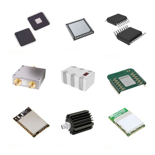
QCC-711-1-MQFN48C-TR-03-1 Bluetooth Audio SoC with MQFN48C Package
-

0339-671-TLM-E Model – High-Performance TLM-E Package for Enhanced Functionality
-
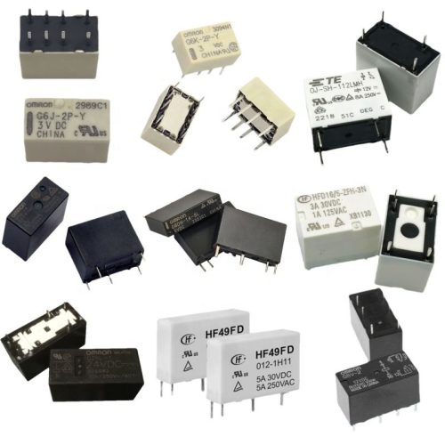
1-1415898-4 Connector Housing, Electrical Wire-to-Board, Receptacle, Packaged
Can this converter handle temperature-sensitive applications?
Yes. It operates from -40??C to 85??C and includes over-temperature protection, ensuring system integrity under demanding environmental conditions.
Does it simplify design layout?
Definitely. The QFN-20 package with integrated power stages minimizes PCB space usage and reduces the number of external components needed in the power path.
📩 Contact Us
Where is this IC commonly used?
It is widely deployed in networking infrastructure, computing modules, and telecom applications where efficient power regulation and space optimization are essential.
How does it compare to discrete step-down regulators?
Compared to discrete designs, TPS53432 offers easier implementation, higher integration, and more efficient thermal handling due to fewer external parts and better layout flexibility.

