Overview: SN74LVC3G14 Triple Inverter with Schmitt-Trigger Inputs
The SN74LVC3G14 from Texas Instruments is a triple Schmitt-trigger inverter designed for noise-resistant digital logic applications. Utilizing CMOS technology, this device combines low static power consumption with high-speed operation, making it ideal for modern systems requiring reliable signal shaping.
Packaged in a space-saving DCT (SSOP-8) form factor, it offers three independent inverters that accept slow or noisy input transitions and convert them into sharp digital outputs. This IC simplifies interface logic and control signal processing across industrial, embedded, and consumer systems.
🔥 Best-Selling Products
-
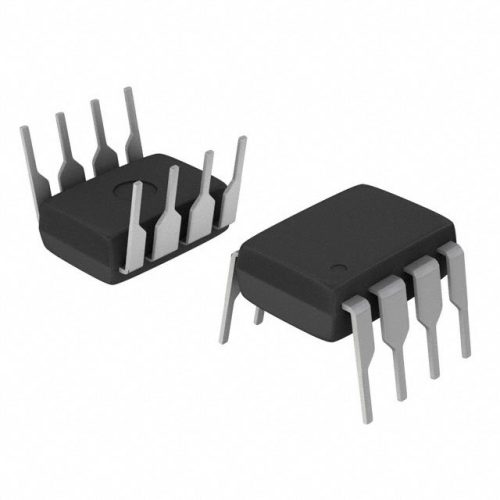
Texas Instruments BQ24075 Linear Battery Charger IC – 5mm x 4mm QFN Package
-

Texas Instruments INA219 Current Sensor Module – SOIC Package, Precision Monitoring
-

Texas Instruments LM4041 Precision Voltage Reference – SOT-23 Package
-

Texas Instruments OPA2134 Audio Op Amp – Dual, High-Performance, SOIC-8 Package
Technical Specifications Table
| Parameter | Min | Max | Unit |
|---|---|---|---|
| Supply Voltage (VCC) | 1.65 | 5.5 | V |
| Input Voltage Range | 0 | 5.5 | V |
| Output Type | CMOS | ?C | |
| Propagation Delay (2V/5V) | 4.6 | 0.9 | ns |
| Package Type | DCT (SSOP-8) | ?C | |
| Operating Temp | -40 | 125 | ??C |
Why SN74LVC3G14 Outperforms Standard Inverter ICs
Compared to conventional inverters, this triple Schmitt-trigger logic gate provides enhanced noise immunity and cleaner signal transitions, especially when dealing with analog-like or slow input edges. Designers benefit from reduced jitter, cleaner logic transitions, and less susceptibility to glitches caused by signal noise. Its flexible VCC range makes it well-suited for both legacy and modern voltage domains. Available at IC Manufacturer, the SN74LVC3G14 reflects the high quality associated with Texas Instruments logic families.
Extended Electrical Characteristics
| Feature | Specification |
|---|---|
| Logic Function | Triple Schmitt-Trigger Inverter |
| Input Compatibility | TTL/CMOS |
| Quiescent Current | Low Static Power |
| Propagation Delay (3.3V) | 1.5 ns |
| Input Hysteresis | Typical 800 mV (at 5V) |
| Temperature Range | ?C40??C to 125??C |
Typical Applications
- Signal conditioning for noisy switches and sensors
- Logic interfacing for industrial control systems
- Debouncing mechanical switches
Frequently Asked Questions (FAQ)
What does the Schmitt-trigger input offer over standard logic gates?
Schmitt-trigger inputs improve noise immunity by incorporating hysteresis, which filters out minor voltage fluctuations and ensures clean, digital transitions even with slowly changing or noisy signals.
🌟 Featured Products
-

“Buy MAX9312ECJ+ Precision Voltage Comparator in DIP Package for Reliable Performance”
-
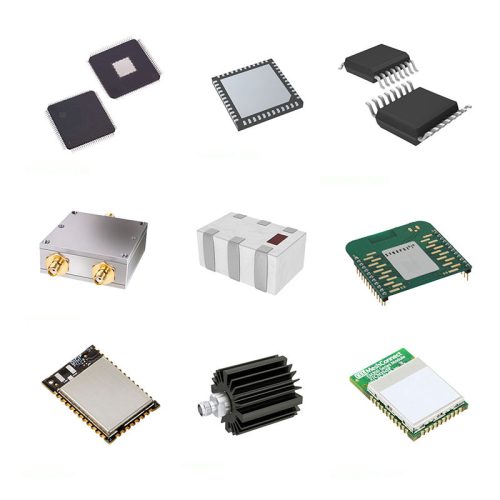
QCC-711-1-MQFN48C-TR-03-1 Bluetooth Audio SoC with MQFN48C Package
-

0339-671-TLM-E Model – High-Performance TLM-E Package for Enhanced Functionality
-
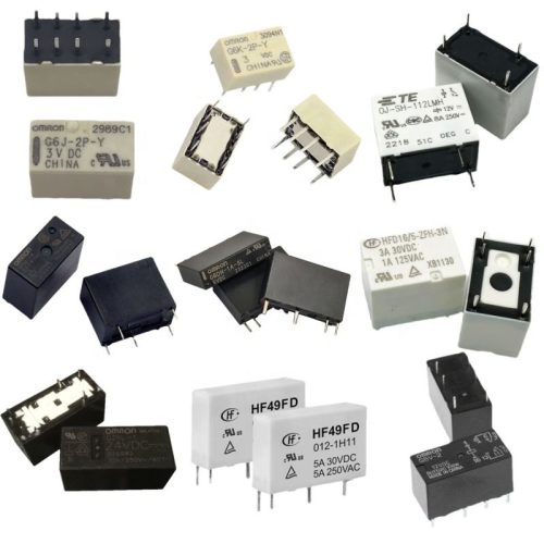
1-1415898-4 Connector Housing, Electrical Wire-to-Board, Receptacle, Packaged
Is the SN74LVC3G14 compatible with both 3.3V and 5V systems?
Yes, the device operates from 1.65V to 5.5V, allowing it to interface directly with both 3.3V and 5V logic families, enhancing its flexibility in mixed-voltage systems.
Can this IC be used in power-sensitive applications?
Yes. Its CMOS architecture ensures very low quiescent current, making it suitable for power-conscious designs like battery-operated or portable electronics.
📩 Contact Us
What applications benefit most from Schmitt-trigger logic?
Applications involving slowly varying inputs, such as analog sensors, long wires, or mechanical switches, benefit most, as Schmitt-trigger gates eliminate glitches and false triggering.
How compact is the DCT (SSOP-8) package?
The DCT package offers a small footprint ideal for high-density layouts in embedded and consumer applications, where board space is at a premium.

