

What Is Winbond 25Q128JVSQ? Features, Specifications, and Sourcing Insights
In embedded hardware, storage is not glamorous.
But it is critical.
A single wrong flash choice can slow boot time, raise power draw, or even break production. That is why the Winbond 25Q128JVSQ remains one of the most widely designed-in SPI NOR flash memories in the world.
This article explains what it is, why it matters, and how to source it safely.
Clear language. Deep detail. Practical insight.
Overview of the Winbond 25Q128JVSQ Flash Memory
The W25Q128JVSQ is a 128-megabit (16 MB) SPI NOR flash memory produced by Winbond Electronics, a global leader in non-volatile memory.
Winbond’s SPI NOR portfolio is known for three things:
- High reliability
- Broad controller compatibility
- Long lifecycle support
Within the 128 Mb family, the 25Q128JVSQ hits a sweet spot.
It balances speed, power, and availability.
For hardware engineers, it is a “safe default.”
For buyers, it is a stable, high-volume part with predictable supply.
As the proverb goes, “Reliability is the foundation of speed.”
— commonly cited in embedded systems engineering circles.
Part Number Breakdown and Ordering Code Explanation
Understanding the part number avoids costly mistakes.
W25Q128JVSQ is not random. Each section carries meaning.
| Code Section | Meaning | Practical Impact |
|---|---|---|
| 25Q | SPI NOR Flash family | Standard SPI/QSPI commands |
| 128 | 128 Mbit density | 16 MB total storage |
| JV | 2.7 V – 3.6 V generation | High compatibility with MCUs |
| SQ | SOIC-8 package | Easy PCB routing |
Suffix comparison (common variants)
| Suffix | Package | Use Case |
|---|---|---|
| JVSQ | SOIC-8 | Prototyping, mass production |
| JVSIQ | WSON-8 | Compact designs |
| JVSIM | SOIC-8 (industrial) | Extended temperature |
Ordering options include tube and tape-and-reel, which directly affect SMT line efficiency.
Core Technical Specifications
This flash is small in size, but strong in capability.
| Parameter | Specification |
|---|---|
| Density | 128 Mbit (16 MB) |
| Interface | SPI, Dual SPI, Quad SPI |
| Supply Voltage | 2.7 V – 3.6 V |
| Max Clock (QSPI) | Up to 104 MHz |
| Operating Temp | –40°C to +85°C (industrial variants available) |
Why Quad SPI matters
Quad SPI (QSPI) uses four data lines instead of one.
That means:
- Faster boot
- Better execute-in-place (XIP)
- Lower active power per byte
For modern MCUs and SoCs, QSPI is no longer optional—it is expected.
Memory Architecture and Erase Granularity
The internal structure is clean and predictable.
| Feature | Value |
|---|---|
| Page Size | 256 bytes |
| Smallest Erase | 4 KB sector |
| Larger Erase | 32 KB, 64 KB blocks |
| Architecture | Uniform sectors |
Why this matters
Uniform sectors simplify firmware updates.
No mixed erase sizes. No surprises.
But there is a rule you cannot break:
You can program bits from 1 → 0, but erase is required to return 0 → 1.
Ignoring this rule leads to corrupted firmware. Every time.

Package Dimensions and Mechanical Specifications
The SOIC-8 (208 mil) package is one reason this part is everywhere.
| Mechanical Feature | Typical Value |
|---|---|
| Body Width | ~5.3 mm |
| Pin Pitch | 1.27 mm |
| Pins | 8 |
| Mounting | Surface-mount |
Advantages of SOIC-8
- Easy hand-soldering
- Low PCB cost
- Strong thermal tolerance
For high-density consumer designs, WSON may win.
For reliability and yield, SOIC-8 still rules.
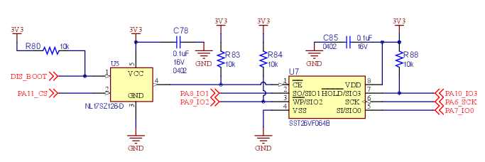
Pinout Description and Signal Functions
The pinout supports both standard SPI and Quad SPI.
| Pin | Name | Function |
|---|---|---|
| 1 | CS# | Chip Select |
| 2 | IO1 | Data I/O |
| 3 | IO2 | Quad Data |
| 4 | GND | Ground |
| 5 | IO0 | Data I/O |
| 6 | CLK | Serial Clock |
| 7 | IO3 | HOLD#/RESET# |
| 8 | VCC | Power |
HOLD# vs RESET#
Older designs use HOLD#.
Modern designs prefer RESET#.
Firmware configuration decides behavior.
Read the datasheet carefully—this pin can save or break recovery modes.
Key Features That Drive Adoption
Why does this part keep getting designed in?
1. High endurance
- Typical 100,000 program/erase cycles
- 20-year data retention at room temperature
2. Fast read performance
- Ideal for boot flash
- Strong support for XIP execution
3. Wide compatibility
- Works with most ARM Cortex-M, RISC-V, and FPGA platforms
- Supported by major boot ROMs and SDKs
In short: it just works.
Power Modes and Low-Power Operation
Low power is not optional anymore.
| Mode | Typical Current |
|---|---|
| Active Read | ~25 mA |
| Standby | ~5 µA |
| Deep Power-Down | <1 µA |
System-level insight
Using deep power-down between events can extend battery life dramatically.
For IoT nodes, this is often the difference between months and years.
As engineers like to say:
“The cheapest power is the power you never use.”
Supply Chain and Sourcing Considerations
This is where many projects fail.
Availability & lifecycle
- Active production
- Long-term industrial support
- Widely stocked by authorized distributors
Sourcing risks
| Risk | Impact |
|---|---|
| Gray market parts | Data corruption |
| Refurbished chips | Early failure |
| Fake date codes | Traceability loss |
Best practices
- Buy from authorized distributors
- Verify date codes and lot traceability
- Avoid “too cheap to be true” offers
In procurement, trust is more valuable than price.
Comparison With Alternatives
| Vendor | Part | Notes |
|---|---|---|
| Winbond | W25Q128JV | Same family, different package |
| Macronix | MX25L128 | Strong alternative |
| GigaDevice | GD25Q128 | Cost-competitive |
| Micron | MT25QL128 | High-end industrial |
The 25Q128JVSQ remains popular because it balances cost, availability, and compatibility better than most.
Final Thoughts: When Is W25Q128JVSQ the Right Choice?
Choose the Winbond 25Q128JVSQ when you need:
- Proven SPI NOR reliability
- Simple PCB layout
- Strong ecosystem support
- Long-term supply confidence
Avoid it only if you need ultra-low voltage, octal SPI, or automotive-grade temperature.
In embedded design, boring is good.
Predictable is better.
And that is exactly what the W25Q128JVSQ delivers.
