MSP430F2252TDA Overview
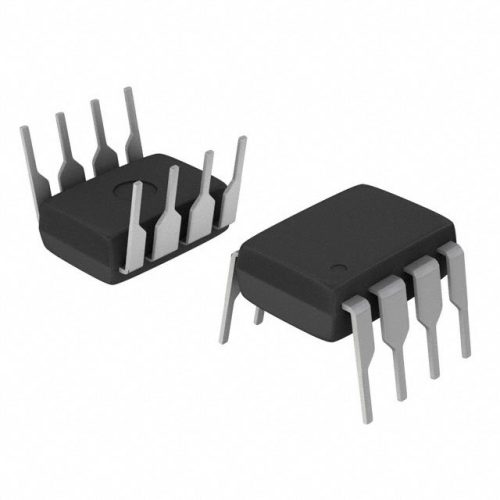
The MSP430F2252TDA is a low-power, 16-bit microcontroller designed for compact industrial and battery-powered systems. It integrates a 16-bit RISC CPU with on-chip nonvolatile memory, a 10-bit analog-to-digital converter, and serial interfaces in a small 20-pin package. The device targets cost-sensitive designs that need more energy efficiency and more deterministic control than generic 8-bit parts. For sourcing and component data, visit IC Manufacturer.
MSP430F2252TDA Technical Specifications
| Architecture | 16-bit RISC CPU |
| Maximum CPU Clock | Up to 16 MHz |
| Flash Memory | 16 KB |
| SRAM | 512 bytes |
| ADC | 10-bit, up to 8 channels |
| GPIO Pins | Up to 16 general-purpose I/O |
| Timers | Timer_A with 3 capture/compare registers |
| Serial Interface | USI/serial module for UART/SPI/I2C functions |
| Operating Voltage | 1.8 V to 3.6 V |
| Package | 20-pin TSSOP / 20-pin VQFN (typical) |
| Power Profile | Ultra-low-power modes for battery operation |
MSP430F2252TDA Key Features
- Single 16-bit CPU core delivering compact code density and more deterministic timing compared with typical 8-bit controllers.
- Integrated Flash memory and on-chip SRAM reduce BOM and simplify firmware updates in production.
- 10-bit ADC with multiple channels provides more accurate sensor readings than many low-cost microcontrollers.
- Low-voltage operation from 1.8 V to 3.6 V enhances compatibility with modern battery chemistries and power rails.
- Flexible serial interface supports UART, SPI, and I2C-like functions for broad peripheral interoperability.
- Timer_A with capture/compare units enables precise PWM and timing control for motor drive and power conversion.
- Compact 20-pin package enables dense board layouts while keeping I/O accessible for sensor and comms tasks.
Typical Applications
- Battery-powered sensor nodes that require ultra-low standby current, precise 10-bit conversions, and minimal BOM cost for long-life installations.
- Portable instrumentation where a 16-bit core and on-chip Flash deliver more algorithm headroom and faster data processing than 8-bit alternatives.
- Industrial control interfaces that need deterministic Timer_A PWM and reliable serial links for motor control or valve actuation tasks.
- Communications gateways that aggregate sensor data using UART, SPI or I2C-style interfaces and forward it to higher-level controllers.
MSP430F2252TDA Advantages vs Typical Alternatives
Compared with mainstream 8-bit microcontrollers, this device provides more processing headroom with its 16-bit core and a higher maximum clock. The on-chip 16 KB Flash and 512 B SRAM reduce external memory needs and speed firmware development. The integrated 10-bit ADC and flexible serial interface lower system cost by avoiding separate converter or comm chips. For battery-first designs, the published low-voltage range and multiple power modes yield better standby energy efficiency than many general-purpose MCUs.
🔥 Best-Selling Products
MSP430F2252TDA Brand Info
This silicon is from Texas Instruments, the vendor behind the MSP430 family of ultra-low-power microcontrollers. The series emphasizes energy efficiency and mixed-signal integration for embedded and industrial designs, with broad toolchain and ecosystem support from the manufacturer.
FAQ
What core does it use?
It uses a 16-bit RISC central processing unit optimized for low-power operation and efficient code density. The core gives more arithmetic and addressing capability than 8-bit alternatives, useful for control and signal-processing tasks.
🌟 Featured Products
-

“Buy MAX9312ECJ+ Precision Voltage Comparator in DIP Package for Reliable Performance”
-

QCC-711-1-MQFN48C-TR-03-1 Bluetooth Audio SoC with MQFN48C Package
-

0339-671-TLM-E Model – High-Performance TLM-E Package for Enhanced Functionality
-

1-1415898-4 Connector Housing, Electrical Wire-to-Board, Receptacle, Packaged
What is the Flash and RAM size?
On-chip nonvolatile storage and SRAM are provided to store application code and runtime data. The integrated Flash enables field firmware updates while SRAM holds stack, variables, and runtime buffers.
Which analog peripherals are available?
The device includes a 10-bit analog-to-digital converter with multiple input channels. This lets designers read sensors with finer resolution than typical low-cost MCUs without adding an external ADC.
📩 Contact Us
What serial interfaces does it support?
It offers a universal serial interface capable of UART, SPI and I2C-like communications. This flexibility allows straightforward connection to sensors, radios, and external memory or peripherals.
What packages can I source?
Common footprint options include compact 20-pin packages such as TSSOP and VQFN variants. These are suited to space-constrained PCBs while still offering accessible GPIO for I/O and peripherals.


