MSP430F1232IDWR Overview
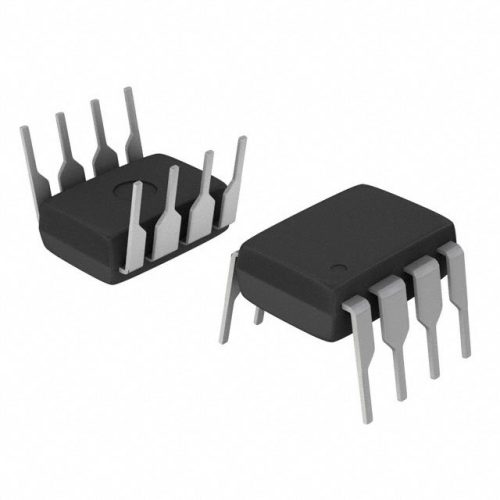
The MSP430F1232IDWR is a low-power, 16-bit microcontroller in the MSP430 family. It balances small-system integration with energy efficiency for battery-powered and embedded industrial designs. The device combines a single 16-bit CPU core with mixed-signal peripherals and on-chip nonvolatile memory to reduce external components and board area. Engineers sourcing compact MCUs will find a clear trade-off between low active power and sufficient peripheral density for control, sensing, and serial communications. See IC Manufacturer for purchasing and distribution options.
MSP430F1232IDWR Technical Specifications
| Parameter | Value |
|---|---|
| CPU core | 16-bit RISC |
| Flash memory | 16 KB |
| SRAM (RAM) | 512 B |
| Operating voltage | 1.8 V to 3.6 V |
| Active clock frequency | up to 8 MHz |
| Timers | 2 ?? 16-bit timer modules |
| ADC | 10-bit ADC, up to 8 channels |
| Digital I/O pins | 16 general-purpose I/O pins |
| Serial interfaces | USI for SPI/I2C; UART capable |
| Package | 20-pin VQFN / TSSOP footprint |
| Temperature range | -40 ??C to 85 ??C |
MSP430F1232IDWR Key Features
- Single 16-bit CPU core with deterministic instruction timing, providing compact control code and efficient arithmetic operations for signal handling.
- On-chip nonvolatile Flash memory (16 KB) reduces external storage and speeds firmware updates for faster time-to-market.
- Low-voltage operation from 1.8 V to 3.6 V supports both standard 3.3 V systems and lower-voltage battery designs for longer run time.
- 10-bit ADC with multiple channels for direct analog sensor interfacing, which lowers BOM cost and improves measurement reliability.
- Two 16-bit timers enable precise PWM generation and event capture for motor control or power-conversion functions.
- Integrated USI serial module for SPI and I2C connectivity, simplifying communication with sensors and external peripherals.
- Compact 20-pin package with up to 16 GPIOs offers dense I/O in small board area, compared with larger 28?C40 pin alternatives.
- Industrial temperature rating (-40 ??C to 85 ??C) ensures reliable operation across a wider thermal range than consumer-grade parts.
Typical Applications
- Battery-powered sensor nodes for industrial monitoring where sub-milliamp standby and 1.8?C3.6 V operation extend field life and reduce maintenance cycles.
- Handheld instruments and portable meters that require 10-bit ADC precision, two timers for signal timing, and compact 20-pin packaging to minimize PCB area.
- Motor control and power-conversion microcontroller tasks that need dual 16-bit timers for PWM and capture plus a low active current profile for energy-sensitive systems.
- Serial sensor interfacing and data aggregation in embedded gateways where USI-based SPI/I2C and UART-capable communication reduce external bridge components.
MSP430F1232IDWR Advantages vs Typical Alternatives
The part offers a tighter integration of mixed-signal peripherals in a smaller package than many 8-bit MCUs, while keeping lower active and standby currents versus higher?performance 32-bit parts. With 16 KB Flash and a 16-bit core, it delivers more computational headroom than basic 8-bit controllers and better power economy than many 32-bit options. The 1.8?C3.6 V range and -40 ??C to 85 ??C rating make it more versatile for portable and industrial products where both voltage flexibility and temperature robustness matter.
🔥 Best-Selling Products
MSP430F1232IDWR Brand Info
The MSP430F1232IDWR is a member of Texas Instruments?? MSP430 microcontroller family. The brand emphasizes ultra-low-power design, robust mixed-signal integration, and long product availability cycles. TI positions MSP430 devices for low-energy sensing, metering, and embedded control applications where efficiency and compactness are critical.
FAQ
What is the CPU architecture?
The device uses a 16-bit RISC CPU architecture. That architecture gives compact code size and predictable cycle timing for deterministic control and efficient arithmetic operations.
🌟 Featured Products
-

“Buy MAX9312ECJ+ Precision Voltage Comparator in DIP Package for Reliable Performance”
-

QCC-711-1-MQFN48C-TR-03-1 Bluetooth Audio SoC with MQFN48C Package
-

0339-671-TLM-E Model – High-Performance TLM-E Package for Enhanced Functionality
-

1-1415898-4 Connector Housing, Electrical Wire-to-Board, Receptacle, Packaged
What power supply range is supported?
Supply operation is specified from 1.8 V to 3.6 V. This range supports both 3.3 V systems and lower-voltage battery-operated designs, improving compatibility across many portable applications.
How much on-chip Flash and RAM are available?
On-chip nonvolatile Flash is 16 KB and SRAM is 512 bytes. This combination supports moderate program sizes and small runtime data buffers typical for embedded control and sensing firmware.
📩 Contact Us
Which analog and timer resources are available?
The MCU includes a 10-bit ADC with multiple input channels and two 16-bit timer modules. These resources enable analog measurement, PWM generation, and event capture for control tasks without external timing ICs.
What package and environmental ratings apply?
The part is available in a compact 20-pin package and is specified for an industrial temperature range from -40 ??C to 85 ??C, making it suitable for fielded products with thermal exposure.


