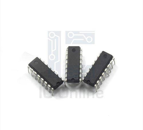
CD5295 Overview
The CD5295 is a versatile integrated circuit designed for precision timing and control applications in industrial and consumer electronics. It offers a robust combination of low power consumption and high operational reliability, making it suitable for a broad range of timing and sequencing tasks. Its architecture ensures stable performance under varying environmental conditions, while its compact design supports efficient board layout. This device is engineered to provide consistent output signals, facilitating seamless integration into complex electronic systems. For detailed technical support and product sourcing, visit IC Manufacturer.
CD5295 Technical Specifications
| Parameter | Specification |
|---|---|
| Supply Voltage (VDD) | 3 V to 15 V |
| Operating Temperature Range | -40??C to +85??C |
| Maximum Output Frequency | 1 MHz |
| Output Current | ??10 mA |
| Power Dissipation | 500 mW (maximum) |
| Input Voltage High (VIH) | 2.0 V (minimum at VDD = 5 V) |
| Input Voltage Low (VIL) | 0.8 V (maximum at VDD = 5 V) |
| Propagation Delay Time | 50 ns (typical) |
CD5295 Key Features
- Wide Supply Voltage Range: Operates reliably between 3 V and 15 V, enabling flexibility across various power environments.
- High-Frequency Operation: Supports output frequencies up to 1 MHz, providing accurate timing for fast switching applications.
- Low Power Consumption: Designed for efficiency, minimizing power dissipation to enhance overall system energy management.
- Robust Temperature Handling: Maintains performance from -40??C to +85??C, ensuring stable operation in harsh industrial settings.
- Fast Propagation Delay: Typical delay of 50 ns allows for precise timing control in sequential circuits.
CD5295 Advantages vs Typical Alternatives
Compared to conventional timing ICs, this device offers superior voltage flexibility and faster propagation delays, which enhance system accuracy and responsiveness. Its extended operating temperature range and low power dissipation contribute to improved reliability and energy efficiency, making it a preferred choice for demanding industrial and automotive applications.
🔥 Best-Selling Products
-
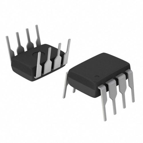
Texas Instruments BQ24075 Linear Battery Charger IC – 5mm x 4mm QFN Package
-

Texas Instruments INA219 Current Sensor Module – SOIC Package, Precision Monitoring
-

Texas Instruments LM4041 Precision Voltage Reference – SOT-23 Package
-

Texas Instruments OPA2134 Audio Op Amp – Dual, High-Performance, SOIC-8 Package
Typical Applications
- Precision timing and sequencing control in industrial automation systems, where stable output signals are critical for synchronized operations.
- Clock generation circuits in embedded systems requiring consistent frequency output over varying supply voltages.
- Pulse generation for signal processing applications in consumer electronics devices.
- Timing control in automotive electronics, where robust temperature tolerance ensures reliable performance under harsh conditions.
CD5295 Brand Info
The CD5295 is part of a product portfolio known for delivering reliable, high-performance semiconductor solutions tailored for industrial and commercial electronics. This IC reflects the brand??s commitment to quality and innovation, providing engineers with dependable components that support efficient design and production cycles. Its reputation is built on rigorous testing and adherence to industry standards, ensuring compatibility and longevity in diverse applications.
FAQ
What supply voltage range does the CD5295 support?
The device operates over a wide supply voltage range from 3 V up to 15 V. This flexibility allows it to be integrated into systems with varying power requirements without compromising performance.
🌟 Featured Products
-

“Buy MAX9312ECJ+ Precision Voltage Comparator in DIP Package for Reliable Performance”
-
QCC-711-1-MQFN48C-TR-03-1 Bluetooth Audio SoC with MQFN48C Package
-

0339-671-TLM-E Model – High-Performance TLM-E Package for Enhanced Functionality
-
1-1415898-4 Connector Housing, Electrical Wire-to-Board, Receptacle, Packaged
What is the maximum operating frequency of this timing IC?
The maximum output frequency supported is 1 MHz, enabling precise timing and switching in high-speed applications such as clock generation and pulse modulation.
How does the CD5295 perform in extreme temperature conditions?
It is rated to function reliably within an operating temperature range of -40??C to +85??C, making it suitable for industrial and automotive environments where temperature variations are common.
📩 Contact Us
What are the power dissipation characteristics of the device?
The maximum power dissipation is specified at 500 mW, which allows for efficient energy use and reduces thermal stress on the circuit, enhancing overall reliability.
How critical is the propagation delay time for applications using this IC?
The typical propagation delay time of 50 ns is important for timing accuracy in sequential logic circuits, ensuring synchronized signal transitions and optimal system performance.


