CD5292 Overview
The CD5292 is a high-performance integrated circuit designed for precision analog signal processing in industrial and consumer electronics. It combines multiple analog functions into a single chip, optimizing space and reducing system complexity. With robust electrical characteristics and a wide operating voltage range, this device ensures reliable operation in demanding environments. Its architecture supports accurate voltage level shifting and buffering, making it suitable for applications requiring stable signal conditioning. Available from IC Manufacturer, the CD5292 offers engineers a versatile solution for enhancing circuit efficiency and integration.
CD5292 Technical Specifications
| Parameter | Specification |
|---|---|
| Supply Voltage Range | 3 V to 15 V |
| Input Voltage Range | 0 V to VDD – 1.5 V |
| Output Voltage Swing | 0 V to VDD – 1.2 V |
| Input Bias Current | Typically 10 nA |
| Operating Temperature | -40??C to +85??C |
| Quiescent Current | 1 mA typical |
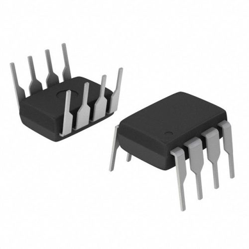
| Package Type | 8-Pin DIP, SOIC |
| Signal Bandwidth | 1 MHz |
| Input Offset Voltage | 5 mV max |
CD5292 Key Features
- Integrated Dual Comparator Functionality: Enables precise voltage comparison for threshold detection, enhancing accuracy in signal processing applications.
- Wide Supply Voltage Range: Operates from 3 V to 15 V, allowing compatibility across various system power levels and improving design flexibility.
- Low Input Bias Current: Minimizes input signal distortion, which is critical for high-impedance sensor interfaces and precision analog circuits.
- High Output Voltage Swing: Provides near-rail-to-rail output, maximizing dynamic range and improving signal clarity in output stages.
CD5292 Advantages vs Typical Alternatives
This device offers enhanced integration by combining dual comparator functions into a compact package, reducing board space compared to discrete solutions. Its low input bias current improves measurement accuracy over typical comparators, while the wide supply voltage range supports diverse applications. These characteristics result in improved system reliability and efficiency, making it a superior choice for precision analog signal conditioning.
🔥 Best-Selling Products
Typical Applications
- Voltage level detection in industrial control systems, where precise threshold monitoring is essential for system safety and performance.
- Battery monitoring circuits requiring accurate voltage comparison to maintain optimal charging and discharging cycles.
- Signal conditioning modules in sensor interfaces, improving signal integrity before analog-to-digital conversion.
- Power management circuits that demand efficient voltage level detection for switching and regulation tasks.
CD5292 Brand Info
Manufactured by a leading semiconductor supplier, this device is part of a well-established family of analog ICs known for reliability and performance. The CD5292 benefits from rigorous quality control and comprehensive technical support, ensuring consistent operation under industrial conditions. Its design emphasizes ease of integration and robustness, catering to engineers seeking dependable analog solutions for complex electronic systems.
FAQ
What is the typical operating voltage range for this device?
The device operates reliably within a supply voltage range of 3 V to 15 V, making it suitable for a wide variety of applications with different power supply configurations.
🌟 Featured Products
-

“Buy MAX9312ECJ+ Precision Voltage Comparator in DIP Package for Reliable Performance”
-

QCC-711-1-MQFN48C-TR-03-1 Bluetooth Audio SoC with MQFN48C Package
-

0339-671-TLM-E Model – High-Performance TLM-E Package for Enhanced Functionality
-

1-1415898-4 Connector Housing, Electrical Wire-to-Board, Receptacle, Packaged
Can the device handle rail-to-rail input and output signals?
While not fully rail-to-rail, the input voltage range extends close to the lower rail at 0 V and up to VDD minus 1.5 V, and the output voltage swing reaches near rail-to-rail levels, offering a wide dynamic range for signal processing.
What package options are available for the CD5292?
The device is offered in standard 8-pin Dual In-line Package (DIP) and Small Outline Integrated Circuit (SOIC) formats, facilitating easy implementation in both prototype and production environments.
📩 Contact Us
How does the low input bias current benefit circuit performance?
Low input bias current, typically around 10 nA, reduces input signal loading and distortion, which is particularly important in high-impedance sensor interfaces to maintain signal accuracy.
Is the device suitable for operation in harsh temperature environments?
Yes, it is specified to operate over a temperature range from -40??C to +85??C, making it suitable for many industrial and commercial applications that require temperature resilience.


