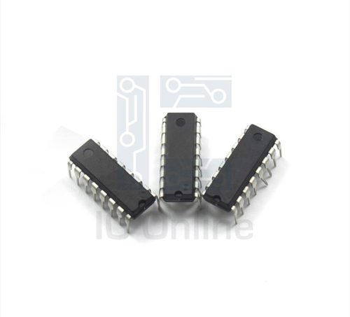
IMLT65R015M2HXTMA1 Overview
The IMLT65R015M2HXTMA1 is a high-performance N-channel MOSFET optimized for advanced power switching applications. Featuring a low on-resistance and robust thermal behavior, it is engineered to deliver reliable efficiency in demanding industrial and automotive environments. Its compact TO-263 package and finely tuned gate charge profile make it ideal for high-frequency switching, power conversion, and load management tasks. For engineers seeking a dependable, low-loss solution, this device stands out for its consistent performance and integration flexibility. Discover more at IC Manufacturer.
IMLT65R015M2HXTMA1 Technical Specifications
| Parameter | Value |
|---|---|
| Device Type | N-Channel MOSFET |
| Maximum Drain-Source Voltage (VDS) | 650 V |
| Continuous Drain Current (ID) | 120 A |
| On-State Resistance (RDS(on)) | 0.015 ?? |
| Gate Charge (Qg) | 194 nC |
| Package Type | TO-263 |
| Operating Temperature Range | -55??C to +150??C |
| Mounting Style | Surface Mount (SMT) |
| Polarity | N-Channel |
IMLT65R015M2HXTMA1 Key Features
- Ultra-low on-state resistance of 0.015 ?? minimizes conduction losses, leading to improved system efficiency in power conversion circuits.
- High drain current capability up to 120 A enables robust support for demanding loads in industrial motor drives and inverter systems.
- 650 V drain-source voltage rating makes it suitable for high-voltage applications, delivering safe operation in harsh environments.
- Optimized gate charge (194 nC) allows for faster switching speeds, reducing switching losses and enabling higher frequency operation.
- TO-263 surface-mount package offers excellent thermal management and ease of integration into compact PCBs.
- Wide operating temperature range ensures reliability in both automotive and industrial temperature extremes.
IMLT65R015M2HXTMA1 Advantages vs Typical Alternatives
Compared to standard MOSFETs, this device delivers superior efficiency through its extremely low on-resistance and high current capability. The combination of high voltage tolerance and optimized gate charge supports both power density and fast switching. Its robust package and broad temperature range further enhance reliability and design flexibility, making it a strong choice for engineers prioritizing performance and durability in power management designs.
🔥 Best-Selling Products
-
Texas Instruments BQ24075 Linear Battery Charger IC – 5mm x 4mm QFN Package
-

Texas Instruments INA219 Current Sensor Module – SOIC Package, Precision Monitoring
-

Texas Instruments LM4041 Precision Voltage Reference – SOT-23 Package
-

Texas Instruments OPA2134 Audio Op Amp – Dual, High-Performance, SOIC-8 Package
Typical Applications
- Industrial power supplies: The device??s high current and voltage ratings make it ideal for use in switched-mode power supplies (SMPS) and power factor correction circuits, where efficiency and thermal performance are critical.
- Electric vehicle inverters: Suitable for traction inverters and DC-DC converters in EVs, leveraging its high switching speed to optimize conversion efficiency and system responsiveness.
- Motor control systems: Its low RDS(on) and high current handling enable reliable operation in industrial motor drives, servo controllers, and robotics applications.
- Renewable energy systems: Used in solar inverters and energy storage interfaces, providing the reliability and power density needed for modern grid-connected and off-grid systems.
IMLT65R015M2HXTMA1 Brand Info
The IMLT65R015M2HXTMA1 is manufactured by a leading global semiconductor supplier renowned for advanced MOSFET technology. This product exemplifies the brand??s commitment to innovation in power electronics, bringing together precise engineering and quality assurance. Designed for demanding industrial and automotive applications, it reflects the manufacturer??s expertise in delivering solutions that meet rigorous safety, efficiency, and integration requirements for next-generation systems.
FAQ
What is the maximum voltage that this MOSFET can withstand between drain and source?
This device is rated for a maximum drain-source voltage of 650 V, enabling it to operate safely in applications with significant voltage stresses and providing headroom for transient events.
🌟 Featured Products
-

“Buy MAX9312ECJ+ Precision Voltage Comparator in DIP Package for Reliable Performance”
-
QCC-711-1-MQFN48C-TR-03-1 Bluetooth Audio SoC with MQFN48C Package
-

0339-671-TLM-E Model – High-Performance TLM-E Package for Enhanced Functionality
-
1-1415898-4 Connector Housing, Electrical Wire-to-Board, Receptacle, Packaged
How does the low on-resistance benefit power designs?
The ultra-low on-state resistance of 0.015 ?? helps minimize power losses during conduction, leading to higher efficiency, reduced heat generation, and lower cooling requirements in high-current power circuits.
Is this device suitable for use in automotive environments?
Yes, the wide operating temperature range from -55??C to +150??C and the robust TO-263 package make it well-suited for automotive applications, where reliability and thermal resilience are crucial.
📩 Contact Us
What are the key considerations for PCB integration?
The surface-mount TO-263 package is designed for straightforward PCB integration, offering good thermal dissipation and compatibility with automated assembly processes, which is essential for high-volume manufacturing.
Can this MOSFET be used in high-frequency switching applications?
With a gate charge of 194 nC and optimized switching characteristics, it supports high-frequency operation, making it a strong candidate for applications like inverters and power converters that demand rapid switching cycles.


