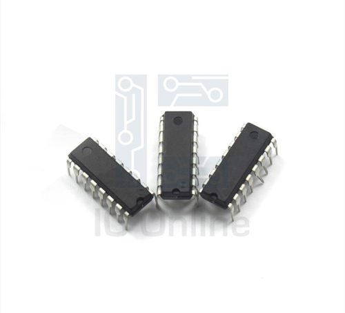
IPD65R225C7ATMA1 Overview
The IPD65R225C7ATMA1 is an advanced N-channel power MOSFET designed to deliver high efficiency and robust switching performance in demanding industrial applications. Utilizing cutting-edge CoolMOS? C7 technology, this device is optimized for low RDS(on) and minimal switching losses, making it ideal for high-frequency power conversion. With a voltage rating of 650V and a compact SMD package, it enables compact, thermally efficient designs. The IPD65R225C7ATMA1 supports engineers in creating reliable, space-saving power electronics with enhanced energy efficiency for industrial and commercial systems. Explore further details at IC Manufacturer.
IPD65R225C7ATMA1 Technical Specifications
| Parameter | Value |
|---|---|
| Drain-Source Voltage (VDS) | 650 V |
| On-Resistance (RDS(on)) | 0.225 ?? |
| Continuous Drain Current (ID) | 7.5 A |
| Gate Charge (QG) | 15 nC |
| Package Type | TO-252 (DPAK) SMD |
| Technology | CoolMOS? C7 |
| Configuration | N-channel |
| Operating Temperature Range | -55??C to 150??C |
IPD65R225C7ATMA1 Key Features
- 650V voltage rating allows safe operation in high-voltage switching environments, supporting robust designs for demanding industrial power supplies.
- Low 0.225 ?? on-resistance significantly reduces conduction losses, which enhances system efficiency and minimizes heat generation for better thermal management.
- Optimized gate charge of 15 nC enables fast switching speeds, improving overall system response and reducing switching losses in high-frequency applications.
- Compact TO-252 (DPAK) surface-mount package streamlines PCB layout and supports automated assembly, saving board space and simplifying thermal design.
- CoolMOS? C7 technology provides minimized dynamic losses, ensuring efficient operation in energy-sensitive systems.
IPD65R225C7ATMA1 Advantages vs Typical Alternatives
Engineered using CoolMOS? C7 technology, this MOSFET offers a superior combination of low on-resistance and reduced gate charge compared to standard silicon MOSFETs. This results in lower conduction and switching losses, supporting higher efficiency and cooler operation. The 650V breakdown voltage and compact DPAK package enable more reliable, space-saving designs for high-voltage and high-frequency applications, setting this device apart from conventional choices.
🔥 Best-Selling Products
-
Texas Instruments BQ24075 Linear Battery Charger IC – 5mm x 4mm QFN Package
-

Texas Instruments INA219 Current Sensor Module – SOIC Package, Precision Monitoring
-

Texas Instruments LM4041 Precision Voltage Reference – SOT-23 Package
-

Texas Instruments OPA2134 Audio Op Amp – Dual, High-Performance, SOIC-8 Package
Typical Applications
- Switch-mode power supplies (SMPS) for industrial equipment, where the high voltage capability and low switching losses improve power density, efficiency, and system reliability.
- Power factor correction (PFC) stages in commercial and industrial power systems, utilizing the fast switching and low RDS(on) to minimize energy loss.
- Motor drive inverters and servo controllers, leveraging the device??s robustness and efficiency to enhance performance and thermal management.
- LED lighting drivers and high-voltage DC-DC converters, benefiting from efficient switching, reduced heat, and compact packaging.
IPD65R225C7ATMA1 Brand Info
The IPD65R225C7ATMA1 is part of a renowned line of high-voltage MOSFETs, built on advanced CoolMOS? C7 process technology. The product is engineered to address the stringent demands of modern industrial and commercial power electronics, offering a blend of low losses, fast switching, and compact form factor. Its reliability and efficiency make it a preferred choice for designers focused on optimizing power management, reducing energy consumption, and achieving consistent performance in challenging environments.
FAQ
What is the primary advantage of using this device in high-voltage power conversion?
The main advantage is its 650V voltage rating combined with low on-resistance and optimized gate charge, allowing for efficient, reliable performance in high-voltage and high-frequency switching applications with reduced losses and improved thermal characteristics.
🌟 Featured Products
-

“Buy MAX9312ECJ+ Precision Voltage Comparator in DIP Package for Reliable Performance”
-
QCC-711-1-MQFN48C-TR-03-1 Bluetooth Audio SoC with MQFN48C Package
-

0339-671-TLM-E Model – High-Performance TLM-E Package for Enhanced Functionality
-
1-1415898-4 Connector Housing, Electrical Wire-to-Board, Receptacle, Packaged
How does the CoolMOS? C7 technology benefit system efficiency?
CoolMOS? C7 technology minimizes both conduction and switching losses by combining a low RDS(on) and low gate charge. This directly translates to higher energy efficiency, cooler operation, and the potential for higher switching frequencies without compromising reliability.
What package type is used, and how does it affect PCB design?
The device is offered in a TO-252 (DPAK) surface-mount package, which allows for automated assembly, efficient heat dissipation, and space-saving PCB layouts??making it ideal for designs where board area and thermal management are critical.
📩 Contact Us
In which typical applications is this MOSFET especially suitable?
This component excels in industrial switch-mode power supplies, power factor correction stages, motor drive inverters, and high-voltage LED drivers, where high efficiency, fast switching, and robust voltage handling are essential requirements.
What is the continuous drain current rating, and what does it mean for system design?
With a continuous drain current rating of 7.5A, the device supports moderate to high load conditions, making it well-suited for demanding switching applications where both current handling and voltage robustness must be balanced for reliable operation.


