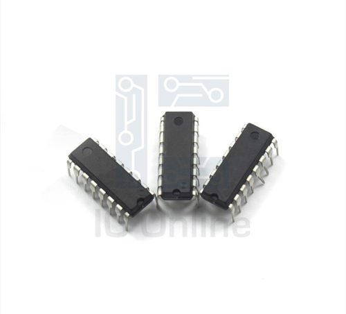
IPP60R190P6XKSA1 Overview
The IPP60R190P6XKSA1 is a high-performance N-channel MOSFET designed to meet the demands of modern industrial and power electronics applications. This device delivers efficient switching and low conduction losses, making it ideal for high-voltage and high-frequency operations. Its advanced silicon technology offers robust performance, enabling reliable operation in demanding environments. With a focus on energy efficiency and system reliability, this MOSFET is a solid choice for engineers seeking to optimize power management and thermal performance. For detailed sourcing and manufacturer information, visit IC Manufacturer.
IPP60R190P6XKSA1 Technical Specifications
| Parameter | Value |
|---|---|
| Transistor Type | N-Channel MOSFET |
| Drain-to-Source Voltage (VDS) | 600 V |
| Continuous Drain Current (ID) | 17.5 A |
| RDS(on) (Max) | 0.19 Ω |
| Gate Charge (Qg) | 63 nC |
| Package / Case | TO-220 |
| Power Dissipation (PD) | 208 W |
| Mounting Type | Through Hole |
| Operating Temperature Range | -55??C to +150??C |
IPP60R190P6XKSA1 Key Features
- Low RDS(on) for High Efficiency: Minimizes conduction losses, reducing power dissipation and enabling compact thermal designs.
- High Voltage Capability: With a 600 V rating, this MOSFET supports demanding industrial and power conversion circuits.
- Robust Power Handling: Supports up to 208 W dissipation, making it suitable for high-load environments and applications requiring sustained performance.
- Optimized Gate Charge: The 63 nC gate charge ensures fast switching speeds, improving overall system responsiveness and reducing switching losses.
- Wide Operating Temperature Range: Operates reliably from -55??C to +150??C, offering flexibility for harsh or variable ambient conditions.
- Standard TO-220 Package: Ensures compatibility with industry-standard layouts and simplifies integration into existing designs.
IPP60R190P6XKSA1 Advantages vs Typical Alternatives
This N-channel MOSFET stands out due to its combination of low on-resistance, high voltage tolerance, and robust current handling. The device??s efficient switching characteristics and large safe operating area contribute to enhanced reliability and reduced energy losses compared to standard alternatives. Its compatibility with common through-hole mounting further eases integration for both new designs and retrofit projects, supporting engineers in demanding applications.
🔥 Best-Selling Products
-
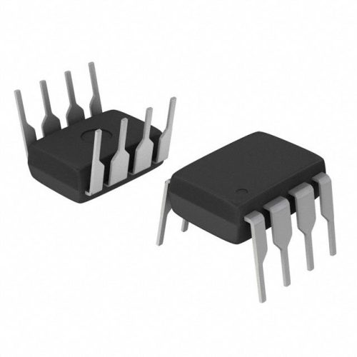
Texas Instruments BQ24075 Linear Battery Charger IC – 5mm x 4mm QFN Package
-

Texas Instruments INA219 Current Sensor Module – SOIC Package, Precision Monitoring
-

Texas Instruments LM4041 Precision Voltage Reference – SOT-23 Package
-

Texas Instruments OPA2134 Audio Op Amp – Dual, High-Performance, SOIC-8 Package
Typical Applications
- Switch Mode Power Supplies (SMPS): The high voltage rating and efficient switching make it well-suited for primary-side and synchronous rectification stages in SMPS, ensuring stable power conversion under varying loads.
- Motor Control Circuits: Its robust current capacity and low conduction losses support precise and reliable motor driver designs for industrial automation and robotics.
- Uninterruptible Power Supplies (UPS): Ideal for high-reliability power backup systems requiring efficient energy flow and robust MOSFETs for protection and switching.
- Lighting Ballasts: Suitable for high-intensity discharge or LED driver circuits, providing efficient and reliable operation in lighting control systems.
IPP60R190P6XKSA1 Brand Info
The IPP60R190P6XKSA1 is designed and manufactured to high quality standards, ensuring consistent performance in industrial and commercial applications. This device leverages advanced MOSFET technology to deliver a balance of efficiency, power density, and ruggedness. The product supports engineers and OEMs with a dependable solution for power switching, conversion, and control, backed by a reputation for reliability and robust engineering in the power semiconductor market.
FAQ
What is the primary benefit of using the IPP60R190P6XKSA1 in high-voltage power applications?
The primary benefit lies in its 600 V drain-to-source voltage rating and low on-resistance, which together enable efficient power switching and reduced energy loss. This makes it especially suitable for demanding high-voltage circuits where both reliability and performance are critical.
🌟 Featured Products
-

“Buy MAX9312ECJ+ Precision Voltage Comparator in DIP Package for Reliable Performance”
-
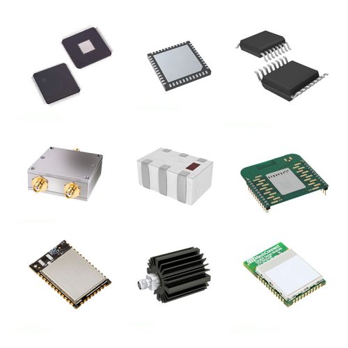
QCC-711-1-MQFN48C-TR-03-1 Bluetooth Audio SoC with MQFN48C Package
-

0339-671-TLM-E Model – High-Performance TLM-E Package for Enhanced Functionality
-
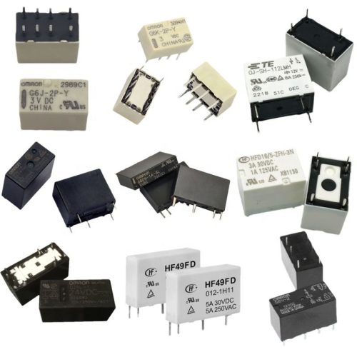
1-1415898-4 Connector Housing, Electrical Wire-to-Board, Receptacle, Packaged
How does the device??s gate charge affect switching performance?
A gate charge of 63 nC allows for fast and responsive switching, which reduces switching losses and improves overall energy efficiency in power conversion applications. Lower switching losses are crucial for applications requiring frequent on-off cycles.
Can the IPP60R190P6XKSA1 operate in harsh temperature environments?
Yes, the wide operating temperature range from -55??C to +150??C allows this MOSFET to function reliably in both extreme cold and hot conditions. This makes it ideal for industrial and outdoor use, where environmental conditions can vary significantly.
📩 Contact Us
What packaging does this MOSFET use, and why is it important?
The device comes in a TO-220 through-hole package. This widely used package style is valued for its thermal performance, ease of mounting, and compatibility with existing PCB designs, making it a practical choice for both prototyping and mass production.
What are some common applications for this device?
Common uses include switch mode power supplies, motor control circuits, uninterruptible power supplies, and lighting ballasts. Its high voltage capability and efficient switching characteristics make it versatile for a broad range of industrial electronics applications.


