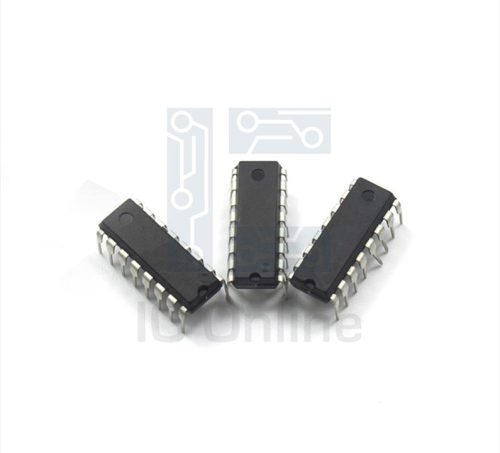
BSS123NH6327XTSA1 Overview
The BSS123NH6327XTSA1 is a compact N-channel enhancement mode MOSFET designed for efficient switching and load control in a wide range of electronic systems. With its low on-resistance and fast switching capabilities, it delivers reliable performance in space-constrained applications. Suitable for use in power management, signal processing, and logic level translation, this device supports robust operation and integration into modern circuit designs. Discover more from IC Manufacturer to ensure optimal component selection for your next project.
BSS123NH6327XTSA1 Technical Specifications
| Attribute | Value |
|---|---|
| Transistor Type | N-Channel MOSFET |
| Package / Case | SOT-23-3 |
| Maximum Drain-Source Voltage (VDS) | 100 V |
| Maximum Continuous Drain Current (ID) | 0.17 A |
| Maximum Power Dissipation | 360 mW |
| On-Resistance (RDS(on)) | 6 ?? at VGS = 10V |
| Gate-Source Voltage (VGS) | ?I20 V |
| Operating Temperature Range | -55??C to 150??C |
BSS123NH6327XTSA1 Key Features
- Low on-resistance ensures minimal power loss, supporting energy-efficient circuit designs.
- High drain-source voltage capability (up to 100 V) enables safe operation in higher voltage environments.
- Compact SOT-23-3 package allows for dense PCB layouts, making it ideal for modern miniature electronics.
- Wide operating temperature range provides reliable performance in various industrial and commercial settings.
- Logic level operation facilitates direct interfacing with microcontrollers and digital logic circuits.
- Fast switching speed supports high-frequency applications, enhancing system responsiveness.
BSS123NH6327XTSA1 Advantages vs Typical Alternatives
This MOSFET stands out for its combination of low on-resistance and high voltage tolerance, leading to improved efficiency and thermal management compared to typical alternatives. Its small SOT-23-3 package maximizes board space utilization, while the wide temperature range and robust electrical ratings provide greater design flexibility and reliability for demanding industrial and commercial applications.
🔥 Best-Selling Products
-
Texas Instruments BQ24075 Linear Battery Charger IC – 5mm x 4mm QFN Package
-

Texas Instruments INA219 Current Sensor Module – SOIC Package, Precision Monitoring
-

Texas Instruments LM4041 Precision Voltage Reference – SOT-23 Package
-

Texas Instruments OPA2134 Audio Op Amp – Dual, High-Performance, SOIC-8 Package
Typical Applications
- Load switching in portable and battery-powered electronics, where compact size and low power loss are essential for maximizing battery life and reliability in mobile devices.
- Signal switching and level translation between logic families or voltage domains in embedded systems, providing seamless connectivity across different circuit sections.
- High-efficiency DC-DC converter circuits needing fast, low-loss switching for power management in industrial or consumer electronics.
- General-purpose switching applications in automation, instrumentation, or test equipment, where robust MOSFET performance is required in space-constrained environments.
BSS123NH6327XTSA1 Brand Info
The BSS123NH6327XTSA1 is produced by a well-established manufacturer recognized for high-quality discrete semiconductors. This device is engineered to meet industry standards for reliability and performance, reflecting a commitment to supporting next-generation electronic designs. The brand??s focus on innovation and quality assurance makes this MOSFET a trusted choice for engineers requiring dependable switching and load control solutions.
FAQ
What is the main benefit of using the BSS123NH6327XTSA1 in compact circuit designs?
Its SOT-23-3 package enables significant space savings on the PCB, making it highly suitable for miniaturized or densely populated electronic assemblies where board area is at a premium.
🌟 Featured Products
-

“Buy MAX9312ECJ+ Precision Voltage Comparator in DIP Package for Reliable Performance”
-
QCC-711-1-MQFN48C-TR-03-1 Bluetooth Audio SoC with MQFN48C Package
-

0339-671-TLM-E Model – High-Performance TLM-E Package for Enhanced Functionality
-
1-1415898-4 Connector Housing, Electrical Wire-to-Board, Receptacle, Packaged
How does its maximum drain-source voltage enhance application versatility?
With a maximum VDS of 100 V, this device can safely handle higher voltage applications, supporting robust switching in both industrial and commercial systems without compromising reliability.
Is the device suitable for direct interfacing with logic-level signals?
Yes, its logic level gate threshold allows for straightforward driving by microcontrollers or digital logic circuits, eliminating the need for additional interface components in many designs.
📩 Contact Us
What thermal performance can be expected from the BSS123NH6327XTSA1?
The MOSFET??s 360 mW power dissipation and wide operating temperature range from -55??C to 150??C support stable operation and effective thermal management, even in demanding environments.
Can this MOSFET be used for both switching and amplification tasks?
While primarily optimized for switching and load control, its electrical characteristics also make it suitable for certain low-power amplification or signal conditioning roles, depending on specific application requirements.


