NLS93333AMR2 Overview
The NLS93333AMR2 is a high-performance semiconductor device designed to deliver precise and reliable operation in demanding industrial and electronic applications. Engineered for efficiency and integration, this product offers a robust set of technical specifications that ensure stable performance under various environmental conditions. Its compact footprint and advanced design make it suitable for applications requiring consistent accuracy and durability. Manufactured by IC Manufacturer, the NLS93333AMR2 stands out as a dependable component for engineers and sourcing specialists aiming to optimize system performance while minimizing maintenance and replacement costs.
NLS93333AMR2 Technical Specifications
| Parameter | Specification |
|---|---|
| Operating Voltage Range | 3.0 V to 3.6 V |
| Operating Temperature Range | -40??C to +85??C |
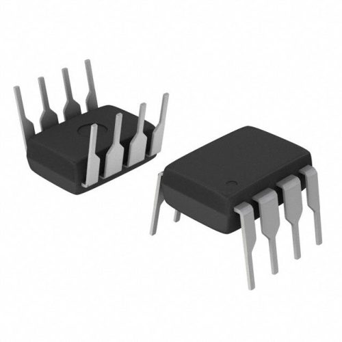
| Package Type | SOP-8 |
| Input Frequency Range | Up to 50 MHz |
| Output Current | Max 20 mA |
| Power Consumption | Typical 1.2 mA |
| Signal Type | CMOS Compatible |
| Response Time | ?? 10 ns |
NLS93333AMR2 Key Features
- Wide voltage operating range: Supports 3.0 V to 3.6 V operation, allowing compatibility with various power supply configurations and ensuring flexibility in system design.
- High-frequency input capability: Handles input frequencies up to 50 MHz, enabling it to function effectively in high-speed digital circuits and communication systems.
- Low power consumption: Typical current draw of 1.2 mA reduces overall system power usage, critical for battery-operated and energy-sensitive applications.
- Fast response time: Response time of less than or equal to 10 ns ensures precise timing control, essential for synchronization in complex electronic systems.
NLS93333AMR2 Advantages vs Typical Alternatives
This device offers superior integration with its SOP-8 package, enabling easier assembly and space savings on PCBs compared to bulkier alternatives. Its wide voltage range and low power consumption provide enhanced energy efficiency and compatibility across varied industrial environments. Additionally, the fast response time and high input frequency handling improve system accuracy and reliability, making it a preferable choice for advanced electronic designs.
🔥 Best-Selling Products
Typical Applications
- Industrial automation systems requiring precise timing and control signals to ensure accurate operation of machinery and process control.
- High-speed communication devices where input frequency handling and fast response are critical for data integrity and transfer rates.
- Battery-powered embedded systems that benefit from low power consumption to extend operational life without compromising performance.
- Consumer electronics needing compact, reliable semiconductor components for signal processing and timing applications.
NLS93333AMR2 Brand Info
Produced by a leading semiconductor manufacturer, the NLS93333AMR2 represents a commitment to quality and performance in the industrial electronics sector. This product is part of a portfolio that prioritizes reliability, precision, and efficiency. The manufacturer applies rigorous testing and quality assurance procedures to ensure each device meets stringent standards, making it a trusted component for engineers and sourcing specialists worldwide.
FAQ
What is the recommended operating voltage range for this device?
The recommended operating voltage range is between 3.0 V and 3.6 V. This range allows stable operation while ensuring the device functions correctly within industrial and commercial power supply standards.
🌟 Featured Products
-

“Buy MAX9312ECJ+ Precision Voltage Comparator in DIP Package for Reliable Performance”
-

QCC-711-1-MQFN48C-TR-03-1 Bluetooth Audio SoC with MQFN48C Package
-

0339-671-TLM-E Model – High-Performance TLM-E Package for Enhanced Functionality
-

1-1415898-4 Connector Housing, Electrical Wire-to-Board, Receptacle, Packaged
Can this device operate in harsh temperature environments?
Yes, it is designed to operate reliably within a temperature range of -40??C to +85??C, making it suitable for harsh industrial environments and outdoor applications where temperature fluctuations are common.
What packaging does the device use, and how does that affect integration?
The component comes in an SOP-8 package, which is a compact and widely used form factor. This packaging facilitates easy integration onto printed circuit boards with standard assembly processes while saving valuable board space.
📩 Contact Us
How does the device??s power consumption impact system design?
With a typical current consumption of 1.2 mA, the product helps reduce overall power demands in electronic systems. This efficiency is particularly beneficial in battery-operated or energy-conscious applications, extending device runtime and reducing heat generation.
Is the device compatible with CMOS logic levels?
Yes, the output signal is CMOS compatible. This compatibility allows seamless interfacing with a wide range of digital ICs and microcontrollers, simplifying system design and reducing the need for additional level shifting components.


