NT2H1311G0DUDZ Overview
The NT2H1311G0DUDZ is a highly integrated, 13.56 MHz NFC Forum Type 2 tag IC designed for contactless data exchange and energy harvesting applications. It features a compact memory size optimized for secure data storage, alongside a robust analog front-end for reliable RF communication. The device supports I2C interface enabling seamless integration into a wide range of embedded systems and smart devices. Its low power consumption and flexible memory organization make it ideal for applications requiring fast, secure, and efficient data transfer. Designed by IC Manufacturer, this solution combines advanced NFC technology with ease of implementation.
NT2H1311G0DUDZ Technical Specifications
| Parameter | Specification |
|---|---|
| Operating Frequency | 13.56 MHz (NFC Forum Type 2) |
| Memory Size | 136 bytes user memory |
| Interface | I2C up to 400 kHz |
| Supply Voltage | 1.8 V to 3.6 V |
| Standby Current | Typically 3 ??A |
| Operating Temperature Range | -40??C to +85??C |
| Package Type | DFN6 2×3 mm |
| Energy Harvesting Capability | Integrated energy harvesting with 2.7 V max output |
| RF Interface | ISO/IEC 14443 Type A compatible |
NT2H1311G0DUDZ Key Features
- Energy Harvesting Functionality: Enables powering of external components by harvesting RF energy from the NFC field, which benefits users by reducing the need for external power supplies in low-power designs.
- Integrated I2C Interface: Allows straightforward connection to microcontrollers and embedded systems, simplifying system design and enabling efficient data exchange.
- Compact Memory with Dynamic Content Management: Provides 136 bytes of user memory organized into dynamically changeable pages, allowing flexible data storage and fast read/write operations.
- Robust RF Communication: Fully compliant with NFC Forum Type 2 and ISO/IEC 14443 Type A standards, ensuring compatibility with a wide range of NFC-enabled devices and readers.
- Low Power Consumption: Operating with minimal current draw during standby and active modes, the device supports energy-efficient applications and extends battery life.
- Small Footprint Package: The DFN6 2×3 mm package minimizes PCB space usage, making it suitable for compact and portable electronic devices.
NT2H1311G0DUDZ Advantages vs Typical Alternatives
Compared to traditional NFC tag ICs, this device offers an integrated energy harvesting feature that reduces external power requirements, enhancing system efficiency. Its combined I2C interface and NFC communication provide flexible connectivity options, improving integration ease. Additionally, the small package size and low power consumption ensure superior reliability and suitability for space-constrained, battery-powered industrial applications.
🔥 Best-Selling Products
-
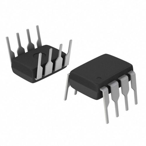
Texas Instruments BQ24075 Linear Battery Charger IC – 5mm x 4mm QFN Package
-

Texas Instruments INA219 Current Sensor Module – SOIC Package, Precision Monitoring
-

Texas Instruments LM4041 Precision Voltage Reference – SOT-23 Package
-

Texas Instruments OPA2134 Audio Op Amp – Dual, High-Performance, SOIC-8 Package
Typical Applications
- Contactless identification and authentication systems requiring secure, fast data exchange with external readers via 13.56 MHz NFC communication.
- Smart sensors and IoT devices that benefit from the energy harvesting capability to power ancillary circuitry without additional power sources.
- Embedded systems needing a compact NFC tag solution with an I2C interface for seamless data transfer and control.
- Portable consumer electronics where low power consumption and minimal PCB footprint are critical design considerations.
NT2H1311G0DUDZ Brand Info
This NFC Forum Type 2 tag IC is part of the NT2H series offered by IC Manufacturer, a recognized leader in semiconductor solutions specialized in contactless communication technologies. The product line is designed to provide reliable, secure, and efficient NFC connectivity for industrial and consumer applications. With a focus on energy efficiency and integration flexibility, this device continues the brand??s commitment to advancing smart connectivity and simplifying system design.
FAQ
What communication protocols does this NFC tag support?
The device supports NFC Forum Type 2 protocol operating at 13.56 MHz and is compliant with ISO/IEC 14443 Type A standards. It also includes an I2C interface for communication with microcontrollers, enabling versatile connectivity options.
🌟 Featured Products
-

“Buy MAX9312ECJ+ Precision Voltage Comparator in DIP Package for Reliable Performance”
-
QCC-711-1-MQFN48C-TR-03-1 Bluetooth Audio SoC with MQFN48C Package
-

0339-671-TLM-E Model – High-Performance TLM-E Package for Enhanced Functionality
-
1-1415898-4 Connector Housing, Electrical Wire-to-Board, Receptacle, Packaged
How does the energy harvesting feature benefit system design?
Energy harvesting allows the device to convert RF energy from an NFC reader into usable power, which can energize external low-power circuits. This reduces or eliminates the need for separate power supplies, simplifying designs and improving overall system efficiency.
What is the typical operating voltage range for this device?
The device operates within a supply voltage range of 1.8 V to 3.6 V, making it compatible with a broad spectrum of low-voltage embedded systems and battery-powered applications.
📩 Contact Us
Can the user memory be dynamically modified during operation?
Yes, the 136 bytes of user memory are organized into pages that can be dynamically read and written over the I2C interface or via NFC commands. This flexibility supports real-time data updates and configuration changes.
What package type is used and how does it impact integration?
The compact DFN6 2×3 mm package minimizes PCB space usage while maintaining robust mechanical and electrical performance. This small footprint is ideal for space-constrained applications and facilitates easier integration into compact device designs.


