ADRF5301BCCZN-RL Overview
The ADRF5301BCCZN-RL is a high-performance, low-noise, I/Q demodulator designed for high-frequency wireless communication systems. This device supports a wide input frequency range, making it ideal for applications requiring precise signal conversion from RF to baseband. Its integrated architecture ensures minimized external components, enhancing system integration and reducing board space. The demodulator provides excellent linearity and low power consumption, making it suitable for advanced radar, communications, and instrumentation equipment. For detailed technical information and sourcing, visit IC Manufacturer.
ADRF5301BCCZN-RL Technical Specifications
| Parameter | Value |
|---|---|
| RF Input Frequency Range | 400 MHz to 4000 MHz |
| IF Output Frequency Range | DC to 200 MHz |
| Conversion Gain | 12 dB (typical) |
| Input Third-Order Intercept Point (IIP3) | +24 dBm (typical) |
| Noise Figure | 11 dB (typical) |
| Supply Voltage | +5 V |
| Power Dissipation | 1.1 W (typical) |
| Package Type | 28-lead LFCSP (4 mm ?? 4 mm) |
| Operating Temperature Range | -40??C to +85??C |
ADRF5301BCCZN-RL Key Features
- Wide RF input frequency range: Supports 400 MHz to 4 GHz, enabling flexible integration in diverse RF systems.
- Low noise figure: Provides 11 dB noise figure for improved signal clarity and sensitivity in demanding applications.
- High linearity: +24 dBm IIP3 ensures excellent distortion performance for accurate signal demodulation.
- Integrated I/Q demodulator architecture: Reduces external component count and simplifies system design.
- Low power consumption: Typical dissipation of 1.1 W supports energy-efficient operation in portable and fixed installations.
- Compact LFCSP package: Enables space-saving PCB layouts without compromising thermal performance.
ADRF5301BCCZN-RL Advantages vs Typical Alternatives
This demodulator offers superior sensitivity and linearity compared to typical alternatives, resulting in more accurate signal processing in complex RF environments. Its wide frequency range and low noise figure improve system performance while maintaining low power consumption. The integrated design simplifies circuit implementation, reduces component count, and enhances reliability, making it a preferred choice for engineers seeking balance between performance and efficiency.
🔥 Best-Selling Products
-
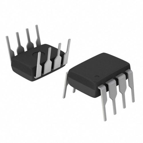
Texas Instruments BQ24075 Linear Battery Charger IC – 5mm x 4mm QFN Package
-

Texas Instruments INA219 Current Sensor Module – SOIC Package, Precision Monitoring
-

Texas Instruments LM4041 Precision Voltage Reference – SOT-23 Package
-

Texas Instruments OPA2134 Audio Op Amp – Dual, High-Performance, SOIC-8 Package
Typical Applications
- Wireless communication systems, including cellular base stations and point-to-point radio links, requiring precise RF to baseband conversion over wide frequency bands.
- Radar signal processing where low noise and high linearity are essential for target detection and identification.
- Test and measurement equipment, facilitating accurate demodulation of complex RF signals for analysis and diagnostics.
- Instrumentation systems needing reliable I/Q demodulation with low power consumption and compact form factors.
ADRF5301BCCZN-RL Brand Info
The ADRF5301BCCZN-RL is part of Analog Devices?? portfolio of RF and microwave components, known for their robust performance in demanding industrial and commercial applications. Analog Devices has engineered this product to meet stringent requirements in wireless infrastructure and instrumentation markets. The company??s commitment to quality and innovation ensures the device delivers consistent performance, reliability, and ease of integration, backed by comprehensive technical support and documentation.
FAQ
What is the input frequency range supported by the ADRF5301BCCZN-RL?
The device supports an RF input frequency range from 400 MHz to 4000 MHz, making it versatile for a broad spectrum of wireless communication and radar applications.
🌟 Featured Products
-

“Buy MAX9312ECJ+ Precision Voltage Comparator in DIP Package for Reliable Performance”
-
QCC-711-1-MQFN48C-TR-03-1 Bluetooth Audio SoC with MQFN48C Package
-

0339-671-TLM-E Model – High-Performance TLM-E Package for Enhanced Functionality
-
1-1415898-4 Connector Housing, Electrical Wire-to-Board, Receptacle, Packaged
How does the noise figure impact the device??s performance?
A noise figure of approximately 11 dB means the device adds low noise to the system, improving overall signal quality and sensitivity, which is critical for detecting weak signals in RF systems.
What are the power requirements for operating this demodulator?
This component operates at a supply voltage of +5 V with a typical power

