JANKCBR2N2221A-Transistor-Die Overview
The JANKCBR2N2221A-Transistor-Die is a precision NPN bipolar junction transistor die designed for high-performance switching and amplification applications. This die offers excellent current gain and robust voltage handling capabilities, making it ideal for integration into custom semiconductor modules and hybrid circuits. With a focus on reliability and thermal stability, it supports efficient power management in compact industrial electronics. Engineers and sourcing specialists benefit from its proven architecture and flexibility within various electronic designs. For more details on sourcing and technical support, visit IC Manufacturer.
JANKCBR2N2221A-Transistor-Die Technical Specifications
| Parameter | Specification |
|---|---|
| Transistor Type | NPN Bipolar Junction Transistor Die |
| Collector-Emitter Voltage (Vce) | 40 V (max) |
| Collector Current (Ic) | 800 mA (max) |
| Gain Bandwidth Product (fT) | 300 MHz (typical) |
| DC Current Gain (hFE) | 100 to 300 (typical) |
| Power Dissipation (Pd) | 625 mW (max) |
| Base-Emitter Voltage (Vbe) | 0.7 V (typical) |
| Junction Temperature (Tj) | 150 ??C (max) |
| Package Type | Bare Die (for hybrid integration) |
JANKCBR2N2221A-Transistor-Die Key Features
- High Current Gain: Enables efficient signal amplification with minimal input drive, which improves overall circuit sensitivity.
- Robust Voltage Handling: Supports collector-emitter voltages up to 40 V, ensuring versatility across various power levels.
- Compact Bare Die Format: Facilitates easy integration into custom semiconductor assemblies, reducing space and improving thermal management.
- Wide Frequency Response: The 300 MHz gain bandwidth product allows for high-speed switching in RF and analog applications.
Typical Applications
- Signal amplification in industrial control systems requiring reliable transistor performance under varying load conditions.
- Switching components in power management circuits for embedded and IoT devices.
- RF amplification stages within communication equipment demanding stable high-frequency operation.
- Custom semiconductor modules and hybrid integrated circuits where space-efficient transistor dies are essential.
JANKCBR2N2221A-Transistor-Die Advantages vs Typical Alternatives
This transistor die offers superior current gain and voltage handling compared to standard packaged transistors, enabling enhanced amplification accuracy and power efficiency. Its bare die format supports direct integration into compact assemblies, improving thermal dissipation and circuit miniaturization. These attributes collectively provide increased reliability and performance consistency in demanding industrial electronics applications.
🔥 Best-Selling Products
-
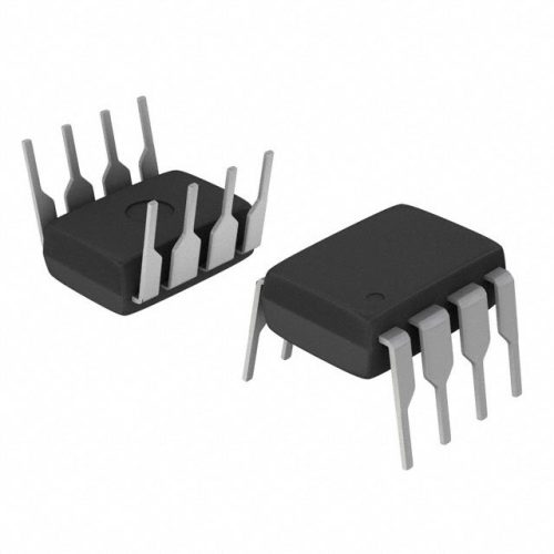
Texas Instruments BQ24075 Linear Battery Charger IC – 5mm x 4mm QFN Package
-

Texas Instruments INA219 Current Sensor Module – SOIC Package, Precision Monitoring
-

Texas Instruments LM4041 Precision Voltage Reference – SOT-23 Package
-

Texas Instruments OPA2134 Audio Op Amp – Dual, High-Performance, SOIC-8 Package
JANKCBR2N2221A-Transistor-Die Brand Info
The JANKCBR2N2221A transistor die is associated with established semiconductor manufacturers specializing in bipolar junction transistor technology. This product line is recognized for quality and durability in industrial and commercial electronic applications. The die form factor indicates a focus on flexible integration into custom and hybrid circuits, favored by engineers requiring precise device customization. For detailed procurement and technical support, consult the original equipment manufacturer or authorized distributors.
FAQ
What are the main electrical characteristics of this transistor die?
The transistor die features a maximum collector-emitter voltage of 40 V, collector current up to 800 mA, and a typical DC gain between 100 and 300. It supports power dissipation up to 625 mW and operates reliably at junction temperatures up to 150 ??C.
🌟 Featured Products
-

“Buy MAX9312ECJ+ Precision Voltage Comparator in DIP Package for Reliable Performance”
-
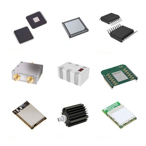
QCC-711-1-MQFN48C-TR-03-1 Bluetooth Audio SoC with MQFN48C Package
-

0339-671-TLM-E Model – High-Performance TLM-E Package for Enhanced Functionality
-
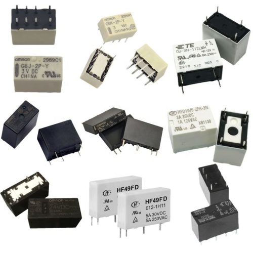
1-1415898-4 Connector Housing, Electrical Wire-to-Board, Receptacle, Packaged
How does the bare die format benefit circuit design?
The bare die format allows for direct integration into hybrid circuits or custom semiconductor packages, enabling designers to save space, optimize thermal management, and tailor the transistor’s placement within the device architecture for improved performance.
Can this transistor die handle high-frequency signals?
Yes, with a gain bandwidth product around 300 MHz, it is suitable for high-frequency switching and amplification, making it effective in RF circuits and other applications requiring fast response times.


